On their own, better tools aren’t enough to keep pace with analog design challenges.

It’s an exciting time to be involved in analog design! Innovation in analog design methodology has been flourishing with the introduction of new tools and improved methodologies. And this innovation is badly needed; analog design is getting tougher. Design schedules remain tight, and the technical challenges analog designers face continue to grow – especially when moving to advanced node technologies. Today’s designers are confronted with:
 Tool developers have been working to keep pace with these requirements. For example, Synopsys has delivered faster circuit simulation performance every year, with improvements in both single core performance and multi-core scalability. And we’ve developed new automation features that reduce custom layout effort. However, tool features on their own are not enough – designers also need to adapt their design methodologies to meet these new challenges.
Synopsys optimizes tool features and design methodologies together through close collaboration with our customers and our own DesignWare IP design team. The DesignWare team is one of the largest mixed-signal design teams in the world, comprising several thousand designers who collectively complete hundreds of designs each year using the Synopsys Custom Design Platform. Two methodology innovations developed through this collaboration have been key enablers for delivering IP at an accelerated pace: early electrical analysis and template-based design re-use.
To speed up analog design closure, designers need to measure parasitics and check for electromigration and IR drop issues during layout. Catching potential electrical issues early can avoid extra design iterations.
An early electrical analysis methodology needs to include three components – electrical constraint specification and verification, on-canvas measurements during layout using signoff quality engines, and simulation using early or partial layout data. The Synopsys analog design methodology integrates these discrete steps into a unified workflow enabling faster design convergence.
As shown in figure 1, an early electrical analysis flow can slash design cycles by providing accurate simulation results long before the layout is complete and LVS clean. In this example, designers could get parasitic simulation results in two hours that were within 5% of the final layout – saving at least a full week of layout time per iteration.
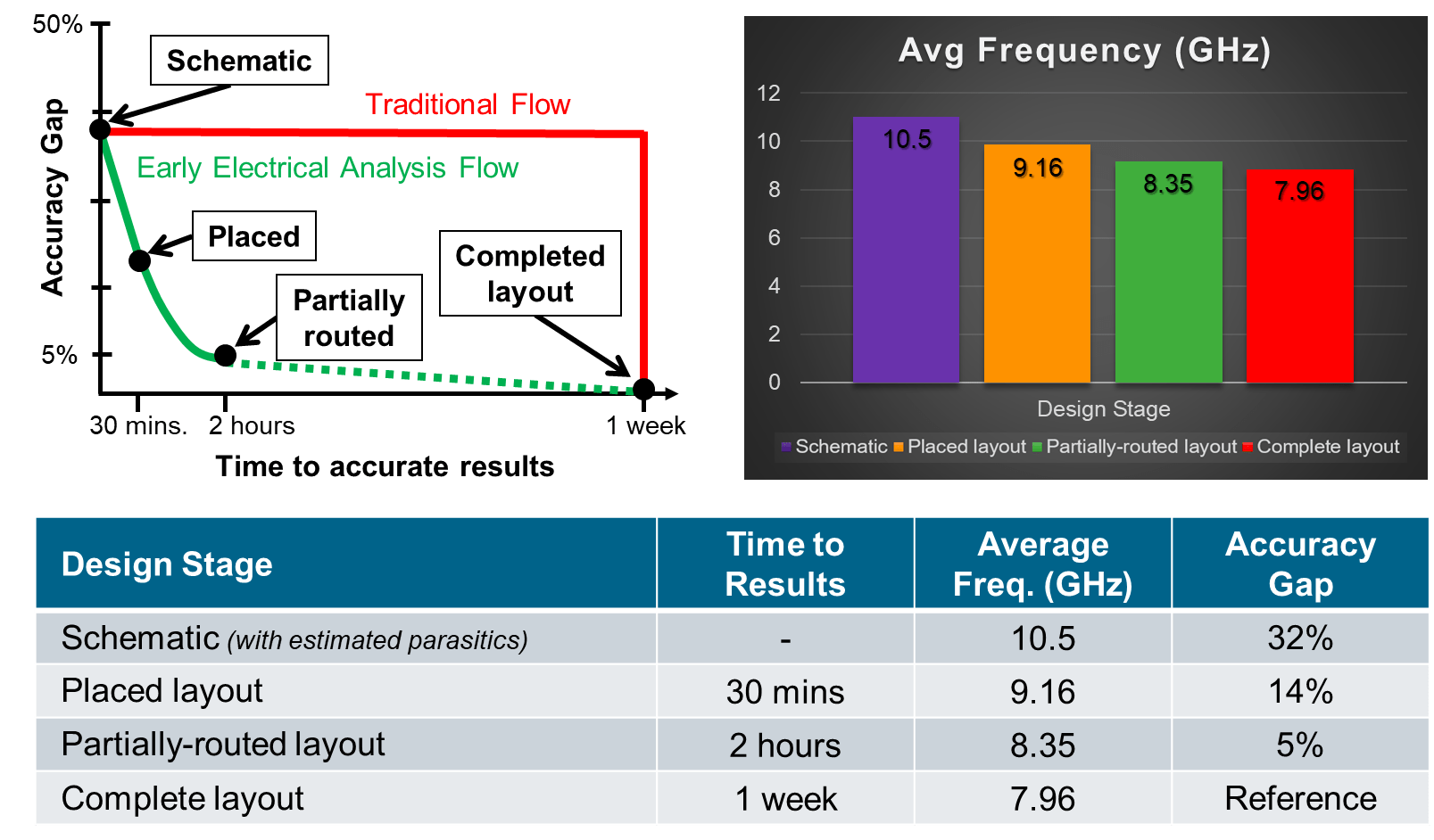
Figure 1: Results from early electrical analysis on example design
One key learning was the importance of using the actual signoff extraction, IR drop and electromigration engines throughout the flow and avoid correlation issues. The Synopsys workflow integrated the signoff StarRC, IC Validator and CustomSim engines in a way that delivered signoff quality results in an interactive setting during a layout creation process.
Analog layout is very demanding, and experienced layout designers are in short supply. A template-based design reuse methodology is a powerful way to leverage the experience of senior designers across the broader layout team.
The same sub circuit topologies recur over and over in analog designs. However, because device sizes in these sub circuits are tailored for the specific needs of the design, it’s not been possible to adopt a cell-based methodology for analog without sacrificing quality of results.
Template-based design is a methodology that leverages the visually-assisted layout automation features in Custom Compiler. Templates extract placement and routing patterns from a layout, including guard rings and dummy devices, and can create new layouts from those patterns using whatever device size the designer needs. Design teams can create template libraries based on the work of senior layout designers for more junior designers to apply. Because templates capture the wisdom and experience embodied in the original design, they make the whole team stronger.
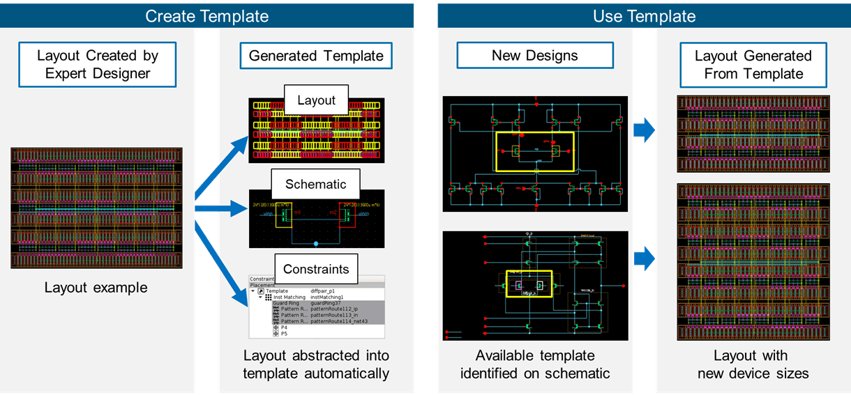
Figure 2: Template-based design re-use
Analog design continues to evolve and drive innovation in every technology area – be that for automotive or 5G or HPC or IoT applications. These have driven shorter design cycle times, use of advanced technology nodes and geographically dispersed teams. Managing analog design deliveries have been increasingly tougher but these challenges have unleashed a fresh wave of innovation. Truly it’s an exciting time to be involved in analog design as these new methodologies and workflows become mainstream.
 |
|
 |
 |
 |
 |
 |
 |
Leave a Reply