Modeling of chip production steps can be a powerful tool to study multi-layer stacking effects and detect hotspots.

By Ruben Ghulghazaryan, Jeff Wilson, and Ahmed AbouZeid
For decades, semiconductor manufacturers have used chemical-mechanical polishing (CMP) as the primary technique for the smoothing and leveling (planarization) of dielectrics and metal layers. CMP modeling allows design and manufacturing teams to find and fix potential planarization issues before the actual CMP process is applied to a wafer. Currently, CMP modeling is widely used for hotspot detection in shallow trench isolation (STI) and back end of line (BEOL) layers as part of a design for manufacturing (DFM) flow (Figure 1).

Figure 1. CMP virtual manufacturing world.
However, critical dimensions of integrated circuits (IC) continuously shrink for each new technology node, imposing more demanding requirements on wafer planarity and depth of focus (DOF) limits. For example, at 20nm, multi-patterning requirements created a whole new set of design constraints to enable successful double-pattterning manufacturing. When gate-last high-k metal gate (HKMG) technology was introduced at the 45nm technology node, two new CMP steps were introduced in the front end of line (FEOL) process flow— poly open planarization (POP) and replacement metal gate (RMG) [1]. At 20nm and below, these two CMP steps are especially critical in forming the gates of transistors, because variation in gate height of just a few atomic layers leads to measurable transistor performance variability [2]. The increasingly high cost of lithography due to multi-patterning, combined with more demanding depth of focus (DOF) requirements and the increased criticality of the HKMG CMP steps, have expanded interest in FEOL CMP modeling at advanced nodes.
Let’s take a look at just what it takes to build an effective FEOL CMP model.
Test chips play a critical role in in the development of accurate CMP modeling, so the first steps in building any new CMP model are to design test patterns and manufacture the test wafers. Restrictive design rules introduced at the 20nm technology node help improve layout unifomity, but make it impossible to use long parallel trenches in array blocks for FEOL CMP. In place of trenches, we created special test patterns for the STI, POP, and Al RMG CMP steps consisting of regular patterns of similarly-oriented rectangles separated by a variety of spacing values in both the horizontal and vertical directions. These different combinations of rectangle sizes and the spaces between them allow a wide variety of density, width, and space combinations for the test patterns. Due to the specific nature of HKMG and Al RMG technology, test chip patterns of POP and Al RMG are correlated. For POP modeling, an inverse (or negative) of the poly layer is used for oxide deposition and polishing, while a positive poly layer is used for the Al RMG step. In Al RMG technology, the sacrificial polysilicon (poly) layer is removed, and the Al layer is deposited instead, then polished. Figure 2 illustrates both of these steps.

Figure 2. Cross section view of Al RMG technology: (a) Polysilicon patterning; (b) Oxide deposition and POP; (c) Poly removal, Al deposition, and polishing.
The next step in CMP modeling is collecting data from the test wafers. Measurements include atomic force microscope (AFM) or other profiler tool scans, and transmission electron microscopy (TEM) or scanning electron microscopy (SEM) cross-section images. These measured data are an important part of the model-building process because CMP modeling doesn‘t consist entirely of polishing models. It also includes deposition models for pre-CMP profile generation. One challenge of building an accurate and complete CMP modeling process is the generation of a pre-CMP profile before polishing.
At 20nm technology and below, gap filling with high-density plasma chemical vapor deposition (HDP-CVD) becomes increasingly challenging, so new deposition technologies have emerged and become standard. Flowable CVD (FCVD), high aspect ratio process (HARP), and enhanced HARP (eHARP) deposition significantly improves the gap-filling capability, which results in denser films with void-free gap-fill-in features with an aspect ratio of 10:1 and more. With modern equipment, it is possible to get high-quality AFM or high resolution profiler (HRP) 2D and 1D scans for post-deposition (pre-CMP) profiles. However, building a physics-based chip-scale model for the post-deposition profile height is still a challenge, due to the complex nature of the multi-stage process.
Post-CMP models capture such effects as dishing and erosion after the CMP process is complete. Since the feature sizes of 20nm FEOL layers are quite small, using line scans to obtain accurate dishing measurement data for post-CMP steps (STI, POP, and Al RMG) is challenging. Due to the high level of noise in AFM line scans after Platen 1, it is hard to obtain clean erosion and dishing signals. The dishing signal is either blurred (due to a large step size of the AFM or other profiler tool), or it is of the same order as noise in measurements. TEM and SEM images provide valuable information, but such measurements are expensive, time-consuming, and have limitations.
Despite these challenges, we achieved significant progress in CMP modeling of FEOL layers, using the Calibre CMP ModelBuilder tool to construct the models, and the Calibre CMPAnalyzer tool to use the models to simulate the layout. The die-scale Calibre CMPAnalyzer tool uses density, width, space, and other geometry grids extracted from the layout design for CMP simulation. A special command supports proper geometry mask transformations and replacements for modeling the Al RMG step, which allows for continuous multi-layer POP and Al RMG layers in CMP simulations.
Analysis of the measurement data showed that post-deposition profile height variation for FEOL layers is quite small, in contrast to electrochemical deposition (ECD) profile variation for BEOL layers. Because of this, we did not expect any significant erosion after the Platen 1 step, an assumption that was confirmed by analysis of AFM line scans. Thus, we can start our modeling with the post-Platen 1 step by assuming a simple model for post-deposition profile (Figure 3).

Figure 3. Cross section view of (a) STI, (b) POP, and (c) AL RMG polishing layers stacking.
This simplification allows users to overcome the difficulties of gathering the accurate measurement data needed for the modeling of post-deposition and post-Platen 1 steps. In addition, the dishing and erosion that are responsible for gate height variation mainly appear during the final CMP step, when two materials (nitride-oxide, Al-oxide, Cu-oxide, etc.) are polished with high selectivity slurry [4]. Measurements show that accurate line scan data can be collected for this final CMP step. Figure 4 shows erosion and dishing data extracted from line scans using the Calibre CMP ModelBuilder product.

Figure 4. Erosion and dishing data extracted from line scans.
CMP modeling is a combination of process data and measurements from actual silicon. The process data includes items such as layer stack thicknesses, downpressure, polishing rates, slurry selectivity, polishing time, and end point detection (EPD) CMP stop conditions. The data are combined with measurements that include erosion, dishing, and thickness data obtained from TEM or SEM images. Figure 5 shows a combined model recipe that includes deposition, etching, polishing steps, and measurement data table.

Figure 5. Measured data table and recipe windows.
Modeling EPD CMP stop conditions is critical in identifying hotspots, since most modern polishing tools use different EPD systems [5]. The Calibre CMP ModelBuilder tool we used supports a variety of EPD CMP stop conditions for simulations. Using this data, it calibrates the CMP model parameters to best fit the measurements for given process conditions.
Before model calibration begins, it is essential to remove outliers from measured data. Due to the noise in measurements, outliers may lead to large calibration errors and misfit. This is especially true when working on technologies at 28nm and below, where the accuracy of the measurements is close to the accuracy limits of profiler tools. In some cases, the level of noise in the data may be of the same order as the erosion and dishing signals. Careful data analysis should be done to exclude outliers from controversial TEM/SEM and line scan measurement data. The following examples show the results of properly calibrated CMP models that used a combination of TEM and line scan data to accurately and correctly fit the measured data.
In Figure 6, the modeling results from the STI CMP model are compared against the TEM and line scan data. The overall trends are captured and demonstrate a nice fit (correlation is 90%). These results are especially positive when you consider that the erosion data is noisy.
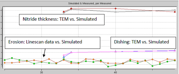
Figure 6. STI CMP model data fitting.
In Figure 7, calibration results are shown for the POP CMP model. Both the erosion and dishing data fit the line scan and TEM data well. Here the fitting correlation exceeds 90%.

Figure 7. POP CMP model data fitting.
In Figure 8, calibration results are shown for the Al RMG CMP model after the final CMP step. Both the gate thickness and erosion data fit the line scan and TEM measurements, with correlation exceeding 90%.

Figure 8. Al RMG CMP model data fitting.
The data presented in Figures 6, 7, and 8 illustrate general fitting trends of model predictions versus simulations. As discussed earlier, using only line scan data is not sufficient for accurate model building, since the extracted values for dishing are limited and the erosion data are noisy. It is also difficult to rely solely on TEM/SEM data, due to the cost and the limited number of TEM/SEM x-section images typically available.
After the model parameters have been calibrated with measurement data from the test chip, the next step is model validation. Model validation requires a comparison of the simulation results to measurements on production designs. Several criteria for validation may be required, depending on the needs of the model users. The most widely-used criteria are the topography trend dependence on pattern density, and metal or oxide thickness value matching with measurements.
To validate the models in our example, we performed several multi-layer STI/POP/Al RMG FEOL CMP simulations on production designs. We then used the Calibre CMPAnalyzer tool to analyze post-CMP topography colormaps and histograms (Figure 9). The analysis shows that the models accurately reveal the correct pattern density versus topography trend. Moreover, our simulations clearly indicate the highest and lowest topography regions (i.e., possible topography hotspots in a design), depending on the planarity requirements.

Figure 9. Colormaps and histogram views for multiple layers help validate the model’s accuracy.
Our simulations revealed that, in some designs, the combined multi-layer STI/POP/Al RMG FEOL CMP simulation hotspots in gate heights may be caused by large profile variations in the STI layer that propagate to the upper layers.
Gate-last HKMG techology introduced a fundamental change in transistor structure and manufacturing flow. It allows gate length scaling and performance of transistors to follow Moore’s law of performance increase, while significantly reducing chip power consumption. Due to the complicated nature of chip design, physical verification, and manufacturing, the modeling of different chip production steps, such as lithography, optical proximity correction (OPC), etch, and CMP, is a powerful and useful tool for both chip designers and process engineers at foundries. Using the CMP model building methodology presented here, we were able to create high-quality STI, POP, and Al RMG FEOL CMP models. The models accurately predicted the measured data from both test chips and production designs. The combined multi-layer FEOL model makes it possible to study multi-layer stacking effects, and provides designers and foundry engineers a powerful solution for detecting hotspots in production designs caused by single-layer or multi-layer design specifics.
[1] K. Mistry, C. Allen, et. al., “A 45nm Logic Technology with High-k+Metal Gate Transistors, Strained Silicon, 9 Cu Interconnect Layers, 193nm Dry Patterning, and 100% Pb-free Packaging“, IEEE International Electron Devices Meeting, Washington D.C., 2007, p 247.
[2] M. Krishnan, J. W. Nalaskowski, and L. M. Cook, “Chemical Mechanical Planarization: Slurry Chemistry, Materials, and Mechanisms“, Chem. Rev. 2010, 110, p 178.
[3] U. Katakamsetty, D. Koli, Y. Sky, H. Colin, R. Ghulghazaryan, B. Aytuna, J. Wilson, “20nm CMP Model Calibration with Optimized Metrology Data and CMP Model Applications“, Proc. of SPIE Vol. 9427, doi: 10.1117/12.2085728, 2015.
[4] R. Ghulghazaryan, J. Wilson, K. Izuha, et al., “Using a Highly Accurate Self-stop Cu-CMP model in the Design Flow“, in Proc. SPIE vol. 7641, 2010.
[5] T. Bibby and K. Holland, “Endpoint Detection for CMP“, Journal of Electronic Materials, vol. 27, No. 10, 1998, p.1073.
Ruben Ghulghazaryan is a lead R&D engineer in the Design to Silicon Division at Mentor Graphics. He has extensive experience in both theoretical and applied physics research, with numerous industry and academic publications. He received a M.Sc. in theoretical physics and biophysics at Yerevan State University and a Ph.D. in physics from Yerevan Physics Institute.
Jeff Wilson is a DFM Product Marketing Manager in the Calibre organization at Mentor Graphics. He has responsibility for the development of products that analyze and modify the layout to improve the robustness and quality of the design. Jeff previously worked at Motorola and SCS. He holds a BS in Design Engineering from Brigham Young University and an MBA from the University of Oregon.
Ahmed AbouZeid is an IC Design Consultant Engineer in the Design to Silicon division of Mentor Graphics, specializing in physical verification. He has hands-on industry and academic experience, with a focus on semiconductor design, physical verification, and EDA tool development, including PDK and fabrication process development. He received a B.S. in Electrical, Electronics, and Communications engineering from Alexandria University, and a M.Sc. in Microelectronics Systems Design from Nile University.
 |
 |
 |
|
 |
 |
 |  |
Leave a Reply