Intel joins DSA consortium; world’s fastest silicon; pushing CMOS.

Intel joins DSA consortium
Arkema, ASML, Intel and others have formed a new consortium in the emerging directed self-assembly (DSA) arena.The group, dubbed PLACYD, is a European funded consortium. Part of the Seventh Framework European Programme (FP7) and funded by ENIAC JU (European Technology Platform for Nanoelectronics), the project includes Arkema, CEA-Leti, STMicroelectronics, Intel, Mentor Graphics, ASML and others.
Led by Arkena, the group is working on a block copolymer materials line to address the necessary building blocks, such as metrology, inspection and design tools, to accelerate the adoption of DSA technology by the semiconductor industry.
It will establish a dedicated material manufacturing facility. With the help of the PLACYD Consortium partners, a dedicated materials line will be set up on the Arkema Research Center site in Lacq, France.
The group will also develop and bring DSA materials to industrial maturity. It will attempt to establish DSA design rules and EDA tools. Metrology and inspection requirements in the sub-10nm range will be defined and implemented in next-generation tools.
World’s fastest silicon
There is a growing interest in developing terahertz-based devices. Target for the sub-mm-wave frequency spectrum, terahertz (THz) devices are geared for military and consumer applications.
These devices range in frequencies from 0.3- to 30-THz. Circuits operating at mm-wave frequencies are typically III-V devices. III-V devices have high mobilities and saturation velocities, but they also have low integration levels and yields.
As a result, the industry is looking to enter the THz-gap spectrum with silicon-based technology. In one step towards reaching that goal, IHP-Innovations for High Performance Microelectronics and the Georgia Institute of Technology have claimed to have demonstrated the world’s fastest silicon-based device. Researchers devised a silicon-germanium (SiGe) device operating at 798-GHz fMAX, exceeding the previous speed record for SiGe chips by about 200 GHz.
IHP designed and fabricated a heterojunction bipolar transistor (HBT) made from a nanoscale SiGe alloy embedded within a silicon transistor. The 800-GHz transistor was made using IHP’s 130nm BiCMOS process.
The operating speeds were achieved at cold temperatures. Researchers demonstrated the device at 4.3 Kelvins. It has a breakdown voltage of 1.7 V.
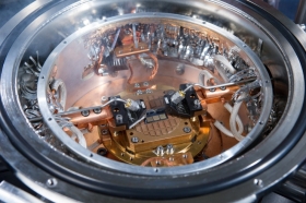
High-speed silicon-germanium chips and measurements probes can be seen inside a cryogenic probe station in a laboratory at the Georgia Institute of Technology. (Georgia Tech Photo: Rob Felt)
“The transistor we tested was a conservative design, and the results indicate that there is significant potential to achieve similar speeds at room temperature–which would enable potentially world changing progress in high data rate wireless and wired communications, as well as signal processing, imaging, sensing and radar applications,” said John Cressler, a professor at Georgia Tech, on the university’s Web site. “Moreover, I believe that these results also indicate that the goal of breaking the so called ‘terahertz barrier’ – meaning, achieving terahertz speeds in a robust and manufacturable silicon-germanium transistor – is within reach.”
Bernd Tillack, who is leading the technology department at IHP, added: “The record low temperature results show the potential for further increasing the transistor speed toward terahertz (THz) at room temperature. This could help enable applications of Si-based technologies in areas in which compound semiconductor technologies are dominant today.”
IHP is part of the so-called DOTSEVEN group, a project supported by the European Commission through the Seventh Framework Programme (FP7) for Research and Technology development. The project is targeting the development of SiGe HBT technologies with cut-off frequencies (fmax) up to 700-GHz. The group will demonstrate the manufacturability and integration with CMOS as well as the capabilities and benefits of 0.7 THz SiGe HBT technology by benchmark circuits and system applications in the 0.1- to 1-THz range.
Pushing CMOS
There has been a tenfold increase in wireless data every four years. If this trend is to continue, 100-Gb/s will be realized around 2020, according to Hiroshima University.
By then, the industry may require THz-based wireless LANs. For low-power applications, CMOS is ideal. Operation frequencies of millimeter-wave CMOS amplifiers have increased twofold every five years.
Pushing the limits with CMOS, Hiroshima University has developed a CMOS transceiver with a carrier frequency of over 100-GHz. A 11-Gb/s wireless data transfer over a distance of 3 meters with a 135-GHz transceiver has been demonstrated based on this design.
A 135-GHz CMOS transceiver was fabricated in a 40nm CMOS process. The areas of the Tx and Rx are 0.44 mm2 and 1.13 mm2 including the pads, respectively. The LNA of the Rx employs a ten-stage CMOS amplifier. The total power consumption is 209 mW, where the power consumptions of the Tx and Rx are 77 mW and 132 mW, respectively. “When trying to obtain the highest possible performance of a MOSFET, the MOSFET must be biased such that its highest fmax is realized,’’ according to researchers from the university. “If, on the other hand, the power consumption is a great concern, one can opt for a reduced-fmax design.”
Meanwhile, Imec is pushing CMOS in a different application. Mm-wave radar systems, featuring a range resolution finer than 10cm and an angular resolution finer than 10 degrees, will be used in next-generation driver assistance systems.
These systems are designed to improve safety in blurry conditions, where image-based driver assistance systems fail. But the high bandwidth and carrier frequency needed to achieve such high resolutions translate into expensive and power hungry mm-wave antenna arrays.
A low-power compact radar technology will be key to enable the application of mm-wave sensors in next-generation applications. In response, Imec, in collaboration with Vrije Universiteit Brussels, have rolled out the world’s first 79-GHz radar transmitter implemented in a 28nm CMOS process.
With an output power above 10dBm, the transmitter front-end paves the way towards a full radar-on-chip solution. Imec’s continuous wave radar transmitter operates in the 79-GHz band. The device has a supply voltage of 0.9V. It consumes 121mW and is compliant with the spectral mask imposed by ETSI. Phase modulation guarantees high resilience against interference and enables code-domain multiple-input, multiple-output (MIMO) radar.
 |
 |
 |
|
 |
 |
 |  |
Leave a Reply