Update on one of the more intriguing technologies for chip-to-chip communications.

By Michael P.C. Watts
At Photonics West, Dow Corning and IBM disclosed a photo-patternable optical interconnect materials set that can support 25 cm interconnect lengths, can be part of a flexible PCB, and survive the industry standard “Telcordia” environmental stress test.
The idea of optical interconnect has been circulating as soon as it was realized that chip to chip communications could be a limit to system processing speed. The industry’s continued success in matching Moores’s law means that fewer chips are needed for a given functionality. In essence, chip to chip delays have been avoided by combining chips. Meanwhile, research has continued to develop optical sources and receivers in silicon with the thought of future need for optical interconnect off chip or within chip.
The group at Dow Corning was given the challenge of making an optically pattern-able flexible waveguide, presumably driven by the latest trend in thin flexible devices. The optical waveguide consists of a patternable core waveguide , and a clad. The clad need a refractive index lower than the core in order to form the waveguide. The refractive index difference is relatively small around 0.02 in order to provide an NA that matches the source. These sort of small index changes are enabeled by simple composition changes. Dow Corning had developed two different polysiloxane materials for core and clad. In this project they had to make the clad flexible and ensure adhesion between all the layers so they can flexed successfully.
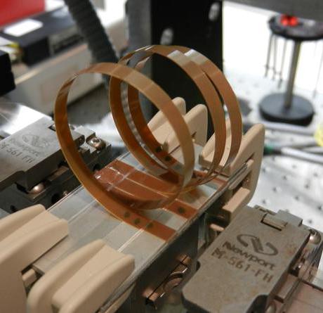
Photo from Dow Corning showing a flexibility test on a waveguide.
The paper at Photonics West disclosed all sorts of test data showing the performance of a 50×50 um waveguide in environmental and mechanical stress tests.
My take is that this sort of testing suggests that optical interconnect PCB at IBM is moving from research into application feasibility testing, which is a significant step towards commercialization.
About the Author
—Mike Watts has been patterning since 1 um was the critical barrier, in other words for a longtime. I am a tall limey who is failing to develop a Texas accent here in Austin. I have a consulting shingle at www.impattern.com.
My blog “ImPattering” will focus on the latest developments in the business and technology of patterning. I am particularly interested in trying to identify how the latest commercial applications evolve.
 |
 |
 |
|
 |
 |
 |  |
Leave a Reply