What’s coming for multi-patterning at 10nm and what you’ll need to know.

I’ve been talking about double patterning for a long time now in this series of blogs. I thought it might be good to start looking ahead at what is next for multi-patterning (Don’t Panic!). As you may have been hearing or reading, it doesn’t look like EUV lithography is going to be ready for 10nm, and may not even make it for 7nm. This means that alternative methods of extending the existing lithography toolset are necessary to keep the industry moving forward.
The 20nm process node first introduced the design community to multi-patterning. The active, contact, via, and lower metal layers began utilizing the Litho-Etch-Litho-Etch (LELE) pitch-splitting double-patterning (DP) process at this node. This is the DP process that all my other blogs have talked about. LELE requires that the DP layers be split (decomposed) into two masks to be manufactured. At some foundries, the designers are required to generate these two decomposed mask layers as part of the tape-out process to the fab. At other foundries, the designers are not required to do the decomposition, but they must run special DP checks to enforce layout restrictions that guarantee the two-layer decomposition is possible once the design is taped out to the fab. In either case, the designers must perform new tasks associated with these layers being split into two masks that were not required for previous nodes.
It is interesting to note that the poly (gate) layer in the 20nm process node also uses two masks, but it is not split in the same way that the LELE process requires for the other DP layers. It uses a line/cut process. The poly layer is restricted to contain uni-directional lines. These lines are all defined using the first “line” mask. Wherever there are gaps (spaces) in the lines, a second “cut” mask is used to define these gaps. Figure 1 shows an example of this line/cut two-mask decomposition.

Figure 1: Example of line/cut two-mask decomposition.
This process is not apparent to the designers, as they do not draw these two masks or perform any type of special decomposition checks for this process. The restrictive design rules of the layer ensure that the generation of these two masks is possible at the fab. Because this dual patterning is essentially “hidden” from the designers, you don’t hear much talk about it.
At the 16/14nm technology node, things appeared to be pretty much the same as they were in the 20nm node in regard to multi-patterning. This consistency was largely because this node was not a true shrink from 20nm to 16/14nm. The interconnect layers stayed the same as they were in 20nm, such that the same DP processes could be used to manufacture them. The only significant change was the new finFET transistor, which is not only a new type of transistor, but also a shrink in size. This transistor requires an entirely new layer (the “fin” layer), in addition to the active and poly layers. This fin layer is essentially a set of parallel lines running perpendicular to the poly layer. It turns out that the pitch (line/space) of these lines also requires some type of DP to be manufactured. The fabs introduced a new DP process, called the spacer-is-mask (SIM), which is a version of self-aligned-double-pattering (SADP). Similar to LELE pitch-splitting and line/cut processes, SIM also requires two masks to manufacture, but the process is very different from LELE or line/cut double patterning. Figure 2 outlines an example of the SIM process.
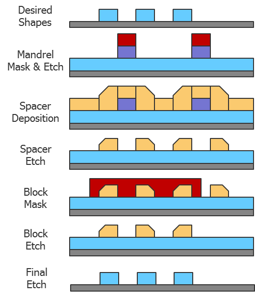
Figure 2: Example SIM SADP process flow used for the fin layer.
As you can see in the process flow diagram, the two masks (“mandrel” and “block”) look very different from the desired final shapes that the designer draws as part of the layout. This disparity is because the final shapes are not defined directly by the mask shapes. The residuals from the spacer deposition and etch serve as the final “masking” pattern. Luckily, for the designer doing 16/14nm layout, the entire generation of the fin layer is hidden. The designer only draws the traditional active and poly (“gate”) layers. Although there are additional restrictions on these layers that were not present in previous nodes, notably that the active layer can only be discrete units of length, these restrictions are enforced with traditional design rules. The severely restricted layout constraints of the layers guarantee that the fab can easily derive the corresponding fin layer needed to complete the new transistor structure.
Moving to the 10nm process node, the changes in multi-patterning will not be so benign to the designer. In addition to all of the techniques used at 16/14nm, the 10nm node introduces at least two new multi-patterning techniques. The first is LELELE pitch-split triple patterning (TP). Yes, when two isn’t enough, why not make it three? This process is very similar to the LELE DP process used at 20/16/14 nm, except that TP requires decomposition of the original layer into three separate masks. Just like DP, when you combine all the shapes (“OR”) from the three masks, it looks like the original single layer again. The TP process may be utilized for layers like contacts, re-distribution interconnect, and/or M1. Figure 3 shows an example of TP decomposition.

Figure 3: Three-mask triple-patterning decomposition.
Because this process is so similar to the 20/16/14nm DP process, designers will find many similarities that may ease the transition to TP. Even the use of fixing solutions like stitching is theoretically available for this process. Figure 4 shows an example layout that is not natively decomposable into three masks, but can be decomposed successfully through the use of stitches.

Figure 4: TP decomposition error corrected using stitching.
As similar as TP may look to DP, many things about it are very different, and it introduces significant challenges to the designer, foundry, and EDA tools. I’ll be investigating some of these challenges in greater detail in upcoming articles.
The 10nm process also introduces the spacer-is-dielectric (SID) version of SADP, which may be used for some of the metal interconnect layers. Like the SIM version of SADP used for 16/14 nm, the two masks do not look like the original drawn shapes in the layout, but utilize the residuals of the spacer deposition and etch process to define shapes. However, in the SID version of SADP, the spacers do not define the lines themselves, but the spaces between the lines. Figure 5 shows an example of a metal process using SID SADP.

Figure 5: SID SADP process for a metal interconnect layer.
Unlike the SIM SADP process used in 16/14 nm for the fin layer, the application of the SID SADP process on a more complex bi-directional layer (like a metal interconnect) does not allow it to be “hidden” from the designer. This process will require some new requirements for the designer to learn and contend with. It also introduces new challenges for the foundry and EDA tools. Don’t worry—I’ll also discuss more about these challenges in upcoming articles. For now, let’s just look briefly at an example metal layout and how it gets decomposed into two masks for this process (Figure 6).

Figure 6: Metal layout decomposed into two masks for SID SADP.
You can see from this example that there are three major steps in the mask decomposition process.
Suffice it to say that you will probably need to engage yourself in some additional multi-patterning education as you look toward beginning any 10 nm design work. Luckily for you, that is what I am here for. At a minimum, I will have plenty to write about for the foreseeable future! I look forward to helping you through the learning curve. For now, let me just leave you with a quick summary list outlining what is introduced at each process node in the multi-patterning realm.
20nm:
16nm:
10nm:
In my next article, we’ll dig a little deeper into triple-patterning. Bring your shovels and gloves.
 |
 |
 |
|
 |
 |
 |  |
I thought the fin was created by the active layer and wasn’t two separate layers. My understating is active defines the isolation trenches that are then filled with oxide. Then a non critical mask is used to define areas where the oxide will be recessed exposing the fins. This article sounds like there is a mufti patterning fin layer?