New lithography, equipment required as packaging continues to scale.

The fan-out wafer-level packaging market is heating up. At the high end, for example, several packaging houses are developing new fan-out packages that could reach a new milestone and hit or break the magic 1µm line/space barrier. But the technology presents some challenges, as it may require more expensive process flows and equipment like lithography.
Fig. 1: Redistribution layers. Source: Lam Research
Today, the industry is developing various types of fan-out packages with different specs and flows. One common spec is the line and space features in the redistribution layers (RDLs). An RDL consists of one or more layers formed on a die, which incorporates copper metal connection lines or traces that are redistributed from one location to the die pads. Line and space refers to the width of the metal traces and the space between them.
As more complex chips are integrated into a fan-out, it may require more layers with finer lines and spaces. For example, today’s fan-out packages range from 5µm line and space (5-5µm) and above with 2-2µm in the works. In R&D, some are working on high-end fan-out technologies at 1-1µm and below, including packages capable of supporting high-bandwidth memory (HBM). Targeted for networking/server applications, fan-out at 2-2µm may appear soon with 1-1µm slated for around 2020.
Amkor, ASE, TSMC and others are developing fan-out packages at or around 1-1µm or below, according to analysts. “Fan-out at such lines and spaces is in the R&D status at several players,” said Jérôme Azémar, an analyst at Yole Développement. “So far, the main target in roadmaps is 2-2µm for standard RDL processes. But by using a fab as a complementary step, it is possible to go even below and reach 1-1µm.”
Azémar is referring to a process step used in both the packaging house and the backend-of-the-line (BEOL) in a fab. But perhaps the biggest change in the fan-out flow involves the lithography equipment, which is used to pattern the RDL trace circuitry, vias and other structures in packages. For fan-out at 1-1µm and beyond, vendors must switch wavelengths and move to i-line or 365nm lithography tools, a move that may add cost and complexity into the equation.
With those issues in mind, the cost-sensitive packaging houses face some tough decisions. For one thing, fan-out at 2-2µm and below is limited to a high-end customer base. And not all customers require fan-out packages at those features, as 5-5µm and above is suitable for most applications.
So do packaging houses make the investments necessary to develop high-end fan-out with an uncertain return, or do they hold off and focus on more mainstream technologies? Packaging houses are weighing options on several fronts. On one key equipment front, they are taking a hard look at the lithography options. For packaging, the mainstream lithography tools are mask aligners and steppers. Then, some vendors are developing newfangled lithographic tools, including laser ablation, as well as direct imaging or maskless lithography systems using multiple beams. Another technology to watch is adaptive patterning.
Packaging trends
An IC package incorporates various interconnect schemes, which connect one structure with another inside a package. The main interconnection technologies are wire bond, flip-chip, wafer-level packaging (WLP) and through-silicon vias (TSVs).
Wire bond stitches one structure to another using tiny wires. In flip-chip, tiny bumps or copper pillars are formed to provide the electrical connections in a package.
At the high end, the industry continues to ramp up 2.5D/3D chips using TSVs, whether those TSVs run through a die or a separate interposer. Interposers incorporate tiny traces to route the electrical connections to the die.

Fig. 2: 2.5D with TSVs and high-bandwidth memory. Source: Samsung
GlobalFoundries, for one, can enable 2.5D designs with interposers at 0.8-0.8µm. “Fine lines and spaces are needed for interposers in 2.5D to enable massively parallel interfaces, such as between processors for networking and graphics and high-bandwidth memory,” said David McCann, vice president of packaging at GlobalFoundries.
2.5D has gained traction in high-end applications, such as FPGAs, graphics chips and networking. But the cost of the interposer and other factors have prevented 2.5D from becoming a more mainstream technology.
Hoping to find a lower-cost solution, the industry is developing a new class of high-end fan-out packages. Vendors continue to develop fan-out for the traditional mid-range space. Because a fan-out doesn’t require an interposer, it is less expensive than 2.5D.
“We are seeing more inquiries for server applications. And we are seeing more interest in using fan-out for server applications,” said John Hunt, senior director of engineering at Advanced Semiconductor Engineering (ASE). “(Customers) want us to be able to do HBM in fan-out. There are two reasons. One, the cost of the interposer is high. Second, you can actually get better electrical performance with fan-out. But you need fine geometries to do that. To route all of the 4,000 I/Os on HBM, especially when you have multiples of them (connected) to the GPUs, you need very fine lines.”
For this, the industry wants to go beyond 2-2µm. “We would like to get down to 1µm at least. That would probably suffice for two or three years. Anything beyond that would be a guess,” Hunt said.
Moving down to 2-2µm and beyond provides several benefits. “You can either reduce the number of RDLs or have high-density interconnects,” said John Lau, senior technical advisor at ASM Pacific Technology. “Of course, this is for high-end products such as supercomputers, servers, telecommunications and networking.”
If the industry can successfully develop high-end fan-out, it could give 2.5D some competition. Generally, though, there could be room for both 2.5D and high-end fan-out in the market.
Fan-out itself is a WLP technology, which involves packaging an IC while it’s still on the wafer. In fan-out, individual dies are embedded in an epoxy material. The interconnects are fanned-out in the package, enabling more I/Os.
There are three main types of fan-out technologies—chip-first/face-down; chip-first/face-up; and chip-last, sometimes known as RDL first.
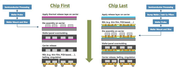
Fig. 3: Chip first vs. chip last. Source: TechSearch International.
The first wave of fan-out packages, called embedded wafer-level ball-grid array (eWLB), appeared in 2009. Today, eWLB packages range from 500 to 1,000 I/Os and use one or two layers of RDL at 10-10µm and below.

Fig. 4: Evolution of eWLB. Source: STATS ChipPAC
Last year, fan-out reached a milestone when Apple adopted the technology for its iPhone 7. Traditionally, Apple and other smartphone OEMs have incorporated a package-on-package (PoP) technology for the application processor. PoP is reliable and cheap, but it runs out of steam at thicknesses of 0.5mm to 0.4mm.
For the iPhone 7, TSMC fabricates Apple’s A10 application processor. Based on a 16nm finFET process, Apple’s A10 is housed in TSMC’s InFO (Integrated Fan-Out). The A10 package thickness ranges from 0.33mm to 0.23mm, according to TechInsights. It uses three layers of RDL at 5-5µm, 10-10µm and 10-10µm, according to sources.
Today, the sweet spot for fan-out is 5-5µm and above. “For mobile or RF products, 10µm line and space is good enough,” said Seung Wook Yoon, director of product technology marketing at STATS ChipPAC. “For the application processor, you may need 7-7µm. The minimum is 5-5µm.”
In R&D, though, the industry is developing high-density fan-out or related packages at 2-2µm and beyond. Last year, for example, ASE introduced a technology called Fan Out Chip on Substrate (FOCoS). Targeted for the server space, the first customer for FOCoS incorporated separate 16nm and 28nm dies in the same package.

Fig. 5: ASE’s FOCoS package. Source: TechSearch International
FOCoS is a hybrid solution based on a fan-out composite die technology. “You put bumps on it. We then treat that as if it was a single die and we flip-chip it onto a BGA substrate,” ASE’s Hunt said. “The basic point is that it eliminates the need for an interposer. It performs electrically better than an interposer.”
The package has four metal layers with 2-2.5µm, although ASE is working on new versions. “We’ve demonstrated 1.5-1.5µm,” he said.
The next step is to move to 1-1µm and beyond, which presents some challenges. Clearly, customers want high-end fan-out packages that meet or exceed the performance of 2.5D at a reasonable price. “Package size is also a challenge since the comfort zone demonstrated for fan-out is still quite small,” Yole’s Azémar said. “Overall, it’s unclear if fan-out will make it in terms of reliability and cost at such high connection densities and package sizes. We will know in one or two years.”
To be sure, though, compared to the current flows, fan-out at 1-1µm and beyond will require different processes and equipment, especially to develop the RDLs.
There are several ways to fabricate the RDLs. The most common and least expensive method is a polymer-based flow. Another method, dubbed the damascene process, is another way to deposit the copper traces in the RDLs.

Fig. 6: A common RDL flow. Source: Chipbond
“If you go down to 2-2µm, we may need a copper damascene or damascene-like process. Even with TSV 2.5D interposers, you need a copper damascene process for 1µm line/space. It’s a different approach from the current wafer-level process,” STATS ChipPAC’s Yoon said.
The biggest and most critical change involves lithography. “The tool needs to be upgraded to meet the requirements,” Yoon said. “Currently, we are using a stepper, which is a broadband source. When you go to finer lines and spaces below 2-2µm, you need i-line.”
It also requires new materials. “We also have to use a different grade of photoresist to make fine linewidth spacing,” he said. “So, the process needs a different litho tool, inspection tool as well as different photoresist materials. I also expect that RDL structure would be a damascene type.”
What is lithography?
Lithography—the art of patterning tiny features on structures—is used in both the fab and packaging house. In the fab, the tools process features at the nanoscale. Meanwhile, in packaging, lithography and other tools are used to process bumps, copper pillars, RDL and TSVs. These structures are measured at the μm level.

Fig. 7: Fan-out equipment and materials forecast. Source: Yole Developpement
In packaging, there are four main lithography equipment types—mask aligners, projection (steppers/scanners), direct imaging, and laser ablation. Mask aligners and steppers are the most common tools, while the other technologies present a threat to the conventional systems.
Used in the industry for years, the mask aligner is the least expensive tool. EV Group and Suss are the main players in the mask aligner business.
In a mask aligner, a wafer moves into the tool. Then, a mask with a set pattern is inserted into the system. The mask is aligned with the wafer and is then exposed with light, forming a pattern on the surface at a 1:1 scale.
Mask aligners are used for processing features at 5-5μm and above, although 3-3μm is possible. “Right now, most people are on 12-12μm or 7-7μm, and are approaching 5-5μm,” said Thomas Uhrmann, director of business development at EV Group. “If you think about eWLB, you can do everything with mask aligners to a big extent.”
Aligners have some limitations, but they are cost effective solutions. “If you want to move into production at 5-5μm or less than 5-5μm line and space, the mask aligner is still perfectly feasible with a superior cost point,” Uhrmann said.
For finer lines and spaces, though, packaging houses use steppers. Ultratech, the leading supplier in the lithography packaging business, sells 1X steppers and other equipment. Other stepper suppliers include Canon, Nikon, ORC, SMEE, Rudolph and Ushio. Recently, Kulicke & Soffa entered the fray by acquiring Liteq, a packaging lithography startup.
A stepper transfers the image of a feature from a mask onto a small portion of the wafer. The process is repeated until the wafer is processed. Some systems process a feature at a scale of 1:1 or 1X. Meanwhile, a reduction stepper images a feature at 2X, 4X or 5X.
A stepper uses different exposure wavelengths to pattern an image. For mainstream applications, packaging houses use traditional steppers that combine several different wavelengths—g, h and i. Generally, this broadband technology is used for patterning at or around 2-2μm and above.
“For greater than 2μm applications, ghi wavelengths (436nm, 405nm and 365nm) are typically used and are usually produced by a broadband spectrum mercury light,” said Rezwan Lateef, vice president and general manager for lithography products at Ultratech.
Beyond 2-2μm, the stepper requires a different configuration. “For 1μm and smaller features, i-line (365nm) only is used to support these fine resolutions,” Lateef said.
Ultratech and others support various wavelengths in the same tool. “You can put a ‘ghi’ wavelength system into an ‘i-only’ mode through the use of an inline filter. This allows the user flexibility to develop recipes to use the most appropriate wavelengths in a seamless, automated fashion,” he said. “So you can use ‘ghi’ wavelength and filter out ‘gh.’ This ability to use selectable wavelengths adds lithography system complexity, but provides the user with flexibility.”
Not all “ghi” tools are alike, however. Some tools are capable of fine lines and spaces, while others struggle to go below 5-5μm, according to analysts.
There are other options. For 2-2μm and beyond, many packaging houses use steppers that are “pure” i-line–they are not shipped with “gh’’ technology. Some i-line steppers are 2X reduction systems that are targeted at 1.5-1.5-μm and below.
Some i-line tools are already processing interposers at 0.8-0.8-μm. “An i-line lithography tool is perfect for this range,” GlobalFoundries’ McCann said.
Regardless of the stepper type, there are several challenges in the packaging flow. For example, “pure” i-line tools are used to process the non-critical layers in a wafer fab. In the fab, the tools process features on flat wafers.
In fan-out, however, it’s a different story. “They are typically reconstituted wafers. They have a lot of warpage. Making sure you have the right depth-of-focus is necessary,” Ultratech’s Lateef said.
Moreover, in fan-out, the dies are embedded in an epoxy mold compound. The placement accuracy of the dies is critical. But at times, the dies move during the process, causing an unwanted effect called die shift. As a result, the fan-out process requires improved alignment techniques with the lithography tools to compensate for die shift.
“The main concerns about smaller geometries in advanced packaging are different depending on wafers or panels,” said Rich Rogoff, vice president and general manager of the Lithography Systems group at Rudolph Technologies. “For both wafers and panels, planarization of the substrates to enable dealing with smaller depth of focus resulting from higher NA is one of the key challenges. Also, tighter registration requirements mean the need for improved alignment and stage systems.”
In one possible solution, Deca Technologies has developed a technology called “adaptive patterning.” The technology is being implemented for its upcoming fan-out line. “One of the challenges within fan-out packaging is the movement of the IC within the reconstituted wafer. Within conventional fan-out packaging processes where masks are employed this misplacement can lead to a lack of interconnect with the bond pad, clearly resulting in a failed unit,” said Garry Pycroft, vice president of sales and marketing for fan-out packaging specialist Deca.
“The adaptive patterning process incorporates an inspection step to determine the shift of the semiconductor within the reconstituted wafer and then adapt the subsequent process steps to handle this shift, thereby resulting in a higher yielding interconnect. The need for adaptive processing becomes even more imperative as you start to work on advanced design rules and multi-die packaging,” Pycroft said.
To be sure, though, cost is also a factor. Prices for a “pure” i-line stepper are higher than a traditional “ghi” system. Therefore, packaging houses need to look at the cost-of-ownership equation. It makes sense to invest in i-line tools if the high-end fan-out market materializes. The risk is that the market never takes off or the products fall short of their expectations.
Other options
Besides steppers, there are other options. For example, Orbotech and Screen Semiconductor Solutions are developing direct imaging systems, which is somewhat like direct-write or maskless lithography.
Screen, also known Dainippon Screen, is targeting its system for the panel-level fan-out market. Meanwhile, Orbotech’s technology is used in the PCB industry. It is also used for IC substrates in packaging.
Orbotech’s laser direct imaging technology uses multiple beams to print features directly on a surface at 8-8μm and below with plans to move to 5-5μm and 2-2μm. “There are many things that you are doing with a stepper for advanced packaging that can be done in a more efficient way with direct imaging,” said Shavi Spinzi, industry marketing director at Orbotech.
Direct imaging has some advantages. “Usually, it’s a multi-beam system in order to meet the right throughput,” Spinzi said. “Instead of using a mask for a stepper or an aligner, you write directly with the laser to form a pattern that you need. Because you don’t use a mask, you can measure the position of the die. And you can, on the fly, calculate the exact positions of the lines you need to draw.”
Another vendor, Suss, is developing another approach called excimer laser ablation. Using 248nm and 308nm wavelengths, Suss’ laser ablation tool enables features at 5-5μm to 2-2μm. Laser ablation can be used in various packaging applications, such as trenches and vias.
Laser ablation is a dry patterning process. The system breaks the molecular structures on the surface. It directly etches the desired circuit pattern.
Laser ablation is promising, but the technology is still immature and needs some work, according to analysts. At the same time, it’s also unclear how far direct imaging will extend.
Clearly, i-line works but cost is a key. All told, packaging houses must find a solution. Otherwise, there is a chance they may miss the high-end fan-out train.
Related Stories
Betting On Wafer-Level Fan-Outs
2.5D, FO-WLP Issues Come Into Focus
2.5D, Fan-Out Inspection Issues Grow
Electroplating IC Packages
 |
 |
 |
 |
 |
 |
 |
 |
Curing is related high temperature during all patterning process and the impact of CTE mismatch between substrate and photoresist hinder the progress of moving finer patterning in multiple Layers.