Technology is being used to examine hard-to-find defects, but speed remains an issue.

E-beam inspection is gaining traction in critical areas in fab production as it is becoming more difficult to find tiny defects with traditional methods at advanced nodes.
Applied Materials, ASML/HMI and others are developing new e-beam inspection tools and/or techniques to solve some of the more difficult defect issues in the fab. E-beam inspection is one of two ways to find defects on a wafer. Optical inspection is the other method. Not long ago, chipmakers mainly used optical tools for defect detection in production. E-beam inspection was only used in R&D, because it is too slow for production.
But as chipmakers move to 16nm/14nm and beyond, the processes have become more complex and the feature sizes are smaller. Moreover, the size of a detectable defect decreases at each node. And an inability to locate these killer defects can impact the yield of a design.
Today, optical inspection remains the workhorse detection tool in the fab, but the technology also is being stretched to the limit in some applications. So chipmakers are moving e-beam inspection into the in-line monitoring flow for some, but not all, applications at 16nm/14nm and beyond.
E-beam inspection is being used to accelerate the yield learning process. In this process, the idea is to find and eliminate one defect type after another until a device can be manufactured according to spec. “In the semiconductor manufacturing industry, the key to success is to complete this learning as rapidly as possible in a process called yield learning. One key strategy to shorten the yield learning cycle is to increase the adoption of in-line defect detection techniques, including e-beam inspection,” said Richard Hafer, senior member of the technical staff at GlobalFoundries, in a paper at the recent ASMC event. (Oliver Patterson, a distinguished member of the technical staff at GlobalFoundries, was the lead author of the paper.)
It’s unlikely that e-beam inspection will completely replace optical in a fab. Optical will remain the high-volume manufacturing (HVM) tool. E-beam is ideal for some defect types and it still has some limitations. Going forward, though, e-beam inspection will be used for more apps in the fab at advanced nodes.
“The e-beam inspection technique is increasingly utilized for the traditional voltage contrast mode (where the non-contact electrical-defect signal can dramatically reduce time to detect), but also for physical defect detection especially in leading-edge technology nodes (7nm, 5nm). It can also be utilized in older technologies (for example 90nm) for physical defects where traditional optical techniques have poor S/N ratios,” according to Hafer and Patterson.
To be sure, e-beam inspection is gaining steam. Here are some of the latest events in the industry:
• ASML/HMI recently introduced an e-beam inspection tool with faster throughputs.
• Applied Materials has developed a technique with an existing tool for cobalt metal lines at 7nm.
• GlobalFoundries and Samsung have separately developed techniques with existing tools that solve some vexing defect issues in finFETs.
• Several companies are developing multi-beam e-beam tools.
What is wafer inspection?
Inspection is the science of finding killer defects in structures. The market for this technology is growing. In 2018, the total patterned wafer inspection market is expected to reach about $1.65 billion, up from $1.43 billion in 2017, according to Bob Johnson, an analyst at Gartner. The figure includes both optical and e-beam.
Of that figure, “the e-beam inspection market was just under $200 million last year,” Johnson said. “It will be around $230 million this year.”
Generally, the two main tool technologies, e-beam and optical, are complementary. Each performs different functions in the inspection flow, and each has some tradeoffs.
An optical inspection tool uses a 193nm light source, advanced optics and sensors to detect defects on a wafer. Optical inspection is primarily used in production, because it is relatively fast. Generally, the throughputs for optical inspection range from one or two wafers an hour.
But optical inspection has some limits in terms of resolutions. The gray area for optical is somewhere between 20nm and 10nm, according to analysts, although vendors continue to push the technology much farther. For example, KLA-Tencor’s 193nm wafer inspection platform, internally called the Gen 5, is being used beyond the so-called grey area.
“Based on the results and customer’s feedback, we expect Gen 5 to continue to support customers in development of 7nm technology, and we see it playing an even larger role on the development and ramp of the 5nm node,” said Rick Wallace, president and chief executive of KLA-Tencor, in a recent conference call.
Unlike optical, which use photons, e-beam leverages the properties of electrons. In simple terms, electrons from an e-beam tool hit and penetrate the surface of a sample. Then, the electrons scatter and bounce back to a detector in the tool. The secondary electrons or backscattered electrons are used to help identify defects in devices.

Fig. 1: E-beam architecture. Source: Applied Materials
E-beam inspection is used to find the smallest defects, as the technology has sensitivities down to 1nm. As before, though, the problem with e-beam inspection is throughput.
Generally, e-beam inspection times are 1,000 times (or more) slower than optical. “E-beam is still orders of magnitude slower than optical inspection, and is not suitable for production monitoring in HVM,” Gartner’s Johnson said.
In operation, an optical tool scans the entire wafer and looks for defects. With e-beam it could take hours, if not days, to scan an entire wafer. But e-beam is ideal in terms of scanning small areas of a die and looking for specific and hard-to-find defects.
For this and other reasons, e-beam inspection was mainly used for engineering analysis in the R&D groups. But that’s beginning to change, at least to some degree.
Not long ago, chipmakers moved from planar devices at 28nm and above to finFETs at 22nm and 16nm/14nm. In finFETs, which are 3D-like structures, the control of the current is accomplished by implementing a gate on each of the three sides of a fin.

Fig. 2: FinFET vs. planar. Source: Lam Research
Detecting defects is challenging for finFETs. For example, defects can get rooted deep or buried into the finFET structures. Tiny bridge defects can occur in pFET structures.

Fig. 3: Difficult to detect small defects in structures. Source: Applied Materials
Then, at each node, the defect sizes become smaller and harder to find. Optical inspection can find many defects, but chipmakers are leaning more on e-beam inspection starting at 16nm/14nm.
“14nm finFET manufacturing technology is able to achieve the highest levels of efficiency, performance and productivity. However, with the constant shrinkage of device dimensions, the detectable defect size drops substantially and makes it extremely challenging to scan with traditional optical inspections due to the limiting factor of the wavelength of light, which is usually on the order of hundreds of nanometers,” said Xing Zhou, metrology application engineer at Samsung’s Austin Semiconductor group, in a presentation at the recent ASMC conference. “The comparative wavelength of e-beam is much smaller than traditional light wavelength, which in turn provides better resolution. Therefore, this technique has been widely used in 14nm in-line defect monitoring.”
E-beam has found a place in the MOL, back-end-of-the-line (BEOL) and other locations for logic. E-beam is also used for and DRAM.
It is not used everywhere in the fab, however. The technology is inserted on a case-by-case basis for select modules in the fab, and used for certain defect problems. “The major defect-of-interests detected by e-beam inspection are embedded defects (physical or electrical), gap defects or systematic patterning defects,” Zhou said.
Both e-beam and optical inspection are geared to find defects, but the two technologies tend to solve different problems. Generally, optical inspection is targeted to find physical defects, such as voids, protrusions and bridges.
E-beam inspection also is used to detect physical defects that are too small for optical. But e-beam is mainly used for electrical or voltage-contrast defect applications, such as electrical shorts and opens, as well as voids in interconnect structures.
In voltage contrast applications, an external bias is applied to a device. Then the e-beam analyzes the variations in the image contrast of the structure to determine if the device is working.
The solutions
Regardless, e-beam inspection is making progress on several fronts. In 2016, ASML Holding entered the e-beam wafer inspection market by acquiring Hermes Microvision (HMI). At the time, HMI was the world’s largest supplier of e-beam wafer inspection tools.
Recently, ASML/HMI introduced their first jointly developed system. It combines HMI’s e-beam tool with ASML’s computational lithography engine.
With the computational engine, ASML is able to model and simulate the reticle features and how they would translate on the wafer. “If you do that, you would already start to identify which areas on the wafer are potentially having a challenge to show up as a hot spot,” said Henk Niesing, director of product management at ASML, in a recent interview. “Then we combine that with all of our sensor data that we have on a scanner. With that, we think we can compute and predict where the patterns will fail.”
The data then is fed into HMI’s e-beam inspection tool. “Basically, (the e-beam tool) will go to these areas on the wafer that already have been identified as potential failures in terms of patterns,” Niesing said. “You don’t have to measure the whole wafer. You can basically identify the areas where there is a potential risk.”
Only a small percentage of the wafer is measured. The rest is analyzed and the hot spots are predicted, thereby speeding up the e-beam inspection process. “It’s a great throughput gain,” he said.
Others are advancing the technology, as well. At the recent IEDM conference, Applied Materials presented a paper on a new application for its e-beam inspection tool. It has found a new way to detect cobalt trench embedded voids in the middle-of-line (MOL) at 7nm.
A chip consists of three parts—the transistor, contacts and interconnects. The transistor resides on the bottom of the structure and serves as a switch. The interconnects, which reside on the top of the transistor, consist of tiny copper wiring schemes that transfer electrical signals from one transistor to another. Those interconnects are becoming more compact at each node, causing an unwanted resistance-capacitance (RC) delay in chips.
Compounding the issues is a relativity new layer called the MOL. The MOL connects the separate transistor and interconnect pieces using a series of contact structures.

Fig. 4: Image of chip with front-end and backend. Source: Wikipedia
The tiny contacts are three-dimensional structures with a small gap. Using a deposition process, the gap within the contact is filled with a conductive tungsten material. This is called a tungsten plug.
At each node, the contact is becoming smaller, so the volume of the tungsten conductor material decreases at each node. That means a signal must flow through a smaller amount of conductive metal. This, in turn, causes a big problem—contact resistance.
To solve this issue, some chipmakers are moving from tungsten to cobalt materials for the plug at 10nm/7nm.
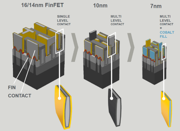
Fig. 5: Cobalt for the MOL at 7nm. Source: Applied Materials
Cobalt reduces the line resistance in chips, but there are some challenges in the cobalt gap-fill process. “The shrinking geometries, in turn, place elevated demands on the metallization process and typical yield-related fail modes include incomplete gap-fill or voiding,” said Nicolas Breil, director of technical projects at Applied Materials, in a recent presentation at IEDM.
So it is critical to conduct a series of inspection steps to verify whether the cobalt gap-fill process was successful or not. For this, defect analysis is sometimes conducted using electrical measurements and a transmission electron microscope (TEM). A TEM has high resolutions, but it is a slow and destructive process. Generally, a sample is cut and then examined in a TEM.
In response, Applied has devised a non-destructive technique using e-beam. But there are several challenges. “As voids in cobalt are usually smaller than the cobalt line width, the detection of voids as small as 5nm is critical,” Breil said. “A spot size smaller than 3nm is required to detect sub-10nm voids.”
To detect voids in cobalt, the electrons from the e-beam must penetrate deep enough in the trenches. In the study, Applied looked at the interactions of an electron beam with energies ranging from 0.5kV to 30kV and depths ranging from 35A to 3.1um.
With e-beam inspection, Applied demonstrated the ability to locate the voids using a mix of energy levels. “When the void is close to the surface (for example, buried under 20nm of cobalt), a relatively small energy gives the maximum contrast. However, when the void is deeper, a higher energy is required. For example, an energy of 20kV is required to generate the maximum contrast and detect voids buried 60nm below the surface. We found a weaker dependency of the size of voids. This means that in order to maximize the detection of voids in cobalt, we have to adapt the beam energy to the required void. Deeper voids require higher energies, while shallower voids favor lower energies,” Breil said.
Meanwhile, some are using e-beam inspection for finFETs. In a recent presentation, for example, Samsung developed a technique to detect shorts in 14nm finFETs.
E-beam can be used to find both open and shorts in devices. Opens are determined using dark voltage contrast (DVC) techniques, while shorts are found using bright voltage contrast (BVC), according to a recent paper from Samsung. DVC signals are easier to validate, but BVC signals are challenging, according to Samsung.
To solve the problem, Samsung devised a BVC technique that involves a separate detection and verification step. The e-beam inspection tool, which is located in the fab, is used for the first step. In simple terms, the e-beam is used to detect an electrical short. But it’s unclear if the signal will fail or not. Then, in the next step, Samsung uses a nano-probing technique, which is the verification step. A nano-probe is a separate failure analysis system that typically resides in a different location called a failure analysis lab.
In nano-probing, tiny tungsten wires are applied on the device to extract electrical parameters. “The leakage current was measured with nano-probing at the BVC (potential fail site) and compared with neighbor normal sites,” Samsung’s Zhou said. “This leakage current based criteria can be used to determine if the BVC signal is a real short or not.”
Then, at that point, a TEM is used to prove that there a short or not. All told, the technique provides “timely information of short fails and helps to accelerate the yield learning cycle,” Zhou said.

Fig. 6: E-beam images of BVC. Source: Samsung
In a separate effort, GlobalFoundries used a nano-probing technique to obtain BVC signals for specific defects in SOI-based finFETs. The goal is to find bright SRAM word-line defects, according to GlobalFoundries.

Fig. 7: Bright gate defect (circled in red) and corresponding FA verification. Three replicates of the same pattern are show in the left image to illustrate how those particular lines look without a short. Source: GlobalFoundries
Generally, nanoprobing is used after a standard TEM failure analysis technique doesn’t find an assignable cause for a group of e-beam inspection defects, according to GlobalFoundries.
In nanoprobing, the tiny probes determine the level of leakage causing the BVC. “Nanoprobing is to land multiple small (~1um diameter) probe tips on conductive nodes on a semiconductor wafer that has been partially or completely processed. Often, the conductive nodes are the drain, source and gate of a suspect transistor, so that its dynamics can be measured and compared to a reference transistor,” according to GlobalFoundries’ Hafer and Patterson. “Using this technique to check voltage contrast defects detected with EBI has become more useful for recent technology nodes because leakages in the nA range have become much more common due to shrinking process margins. Leakages in this range look exactly the same as hard shorts but may not cause hard failure. Understanding if an EBI VC defect is a hard short or leakage is very important for determining the corrective path. Which transistor to probe is determined by counting from a known reference point such as the corner of an SRAM block.”
Where is multi-beam?
While e-beam inspection is making inroads, the technology will never dominate the inspection landscape simply because it’s too slow. So in R&D, the industry has been working on multi-beam e-beam inspection. Using multiple beams, the technology could speed up the throughputs.
In multi-beam, though, the electrons tend to disturb each other, thereby impacting the performance of the tool. The inability to control the electrons is why multi-beam inspection is taking longer to commercialize.
Still, the industry is making progress. ASML, KLA-Tencor and others are developing new multi-beam e-beam inspection technologies for EUV mask inspection. In addition, Zeiss has developed a 91-beam scanning-electron microscope for EUV mask inspection/validation.
Mask inspection is a different application than wafer inspection. If the industry can master multi-beam for mask inspection, it could pave the way towards a similar technology for wafer inspection. Some believe multi-beam wafer inspection tools may appear by 2020. Most, if not all, want them sooner than later.
Related Stories
E-beam Vs. Optical Inspection
Searching For EUV Mask Defects
Overlay Challenges On The Rise
Variation Spreads At 10/7nm
Can We Measure Next-Gen FinFETs?
 |
 |
 |
|
 |
 |
 |  |
Great in-depth article! Every time I came up with a question, the next paragraph answered it. Too bad all the inspection solutions are so slow!
The technology to detect VC defects such as BVC is exactly that of ASML HMI.
Hi Ivan, Here’s my last article on e-beam inspection:
Finding Defects With E-Beam Inspection
https://semiengineering.com/finding-defects-with-e-beam-inspection/
Thank you for sharing this in depth look at eBeam inspection. I have worked with few eBeam tools and companies including AMAT, KLA, HMI and PDF.
Nearly of the eBeam tools are blind scans except PDF solutions tool.