Extending NOR below 28nm may not happen; automotive impact unclear.

Embedded nonvolatile flash memory has played a key role in chips for years, but the technology is beginning to face some scaling and cost roadblocks and it’s not clear what comes next.
Embedded flash is used in several markets, such as automotive, consumer and industrial. But the automotive sector appears to be the most concerned about the future of the technology. Typically, a car incorporates a number of microcontrollers (MCUs) that perform the processing functions in the chip. In many cases, MCUs integrate embedded nonvolatile flash based on NOR technology, which handles the code storage functions. Not all MCUs/processors incorporate embedded flash in the car, however.
MCUs with embedded flash based on 40nm processes and above are widely used in today’s cars. Now, the industry is ramping up 28nm MCUs, which are geared for the instrument cluster, power train and other parts of the vehicle. Carmakers are expected to use MCUs based on 28nm and above for the next several years.
Still, OEMs are weighing the next-generation options and that’s where they face some potential roadblocks. Simply put, it’s difficult to scale NOR flash devices and the embedded version of the technology beyond 28nm. “You will see the bulk of microcontrollers shipped using 130nm or larger process geometries. Those are perfectly fine with embedded NOR,” said Jim Handy, an analyst with Objective Analysis. “The thing that is driving people to change right now is that they haven’t figured out how to do NOR processes smaller than 28nm.”
The industry has known about these issues for some time and is working on several solutions in R&D. But the industry will need to come up with solutions sooner than later amid the shift towards more advanced vehicles with assisted and autonomous driving. The main issues:
• Embedded flash will scale to 28nm and perhaps 22nm. Some are working on scaling the technology to 16nm/14nm, although many believe it will hit the wall at 28nm/22nm.
• If embedded flash runs out of steam, OEMs likely will move the code-storage functions to an standalone NOR device. So instead of one device, OEMs would require a two-chip solution—an MCU and a NOR device.
• Instead of a two-chip solution, OEMs can put the separate MCU and NOR devices in a package.
• MRAM, a next-generation memory type, is being touted as a replacement for embedded flash and cache applications. MRAM works in consumer applications, but it’s still unclear if it will ever meet the temperature requirements for automotive. Some say MRAM will never work in automotive.
To be sure, automotive is different than most markets. In the commercial sector, there is a certain tolerance for defects in chips with a wide range of temperature requirements. In automotive chips, though, there is no tolerance for defects or failures. Plus, there are rigid temperature specs.
More chips in cars
Nonetheless, the automotive chip market is hot. On average, the electronics content per car is expected to climb from $312 in 2013 to $460 in 2022, according to IHS. In total, the automotive IC market is projected to reach a record high of $32.3 billion in 2018, up 18.5% from 2017, according to IC Insights. In automotive, analog is the biggest market with a 45% share, followed by MCUs with 23%, according to the firm.

Fig. 1: Automotive IC market growth. Source: IC Insights
That’s just part of the story, particularly for MCUs. “As sensors and additional MCUs for the automotive environment are deployed, the need for embedded flash is increasing in both number of devices and also with regard to memory density,” said David Hideo Uriu, product marketing director at UMC. “The need for MCUs with embedded flash, as well as other ASICs, will increase as sensor and sensor arrays are implemented within the automotive space to enhance functions related to safety, assisted driving, load-related sensors and infotainment.”
Today’s entry-level cars incorporate some 20 MCUs. Midrange models have 60 MCUs, and luxury vehicles have up to 110, according to Infineon and Strategy Analytics. A 2016 German luxury model has about 25 32-bit MCUs, while the remaining ones are 8- and 16-bit chips, according to the firms.
MCUs incorporate embedded flash, based on EEPROM or NOR. Both provide code storage, which boots up a device and allows it to run programs. “The difference between EEPROM and NOR is whether it has one transistor per bit cell (NOR) or two (EEPROM),” Objective Analysis’ Handy said.
Besides MCUs, carmakers also use standalone NOR devices. Regardless, there are several types of NOR architectures. For example, Silicon Storage Technology (SST), a subsidiary of Microchip, offers embedded flash based on floating-gate technology. In floating gate, the charge is stored in the gate. In addition, Cypress and Renesas offer MCUs based on charge-trap technology, where the charge is stored in the nitride layer of a stack. Meanwhile, NXP and Infineon sell MCUs with different embedded technologies.
Cars, of course, also incorporate other memory types, such as DRAM and NAND. “In 2017, the average memory content per car totaled $21. This number represents total automotive memory sales divided by total vehicles sold in 2017. It only accounts for discrete memory not including embedded memory,” said Jim Feldhan, president of Semico Research.
“Memory content per vehicle varied from a very small amount per car to as much as 8GB of DRAM and 8GB of NAND for L1 and L2 type vehicles,” Feldhan said. “Today, the number of cars equipped with autonomous driving capabilities is low. But autonomous driving applications are growing and the memory content required to enable these applications increases the need for all types of memory. By 2021, a vehicle with L3 automation will require 16GB DRAM and 256GB NAND and by 2025, a fully autonomous vehicle (L5) is expected to require 74GB DRAM and 1TB NAND.”
Regardless, all suppliers of automotive chips face some challenges. “You can’t have parts fail because it impacts safety,” said Robert Cappel, senior director of marketing at KLA-Tencor. “So you’re seeing a much different level of quality and yield. There also is a focus on latent reliability defects. A part may pass a test but fail over time within a car. The requirements are changing.”
New options
In vehicles, meanwhile, MCUs are used in embedded computers called electronic control units (ECUs). ECUs control the various domains in a vehicle, which are connected via a network. ECUs also incorporate other types of chips, such as processors and system-on-chips (SoCs), depending on the application.
Generally, the industry divides a car into five domains—body, connectivity, fusion/safety, infotainment, and power train. Body involves the control of the doors, lighting and windows. Connectivity consists of the cellular, WiFi and related capabilities.
Fusion/safety consists of cameras and radar. Infotainment involves driver information and entertainment. And the powertrain includes engine control and the transmission.

Fig. 2: Semiconductor functions in automobiles. Source: UMC
Each domain has different requirements. For example, the fusion/safety domain will likely use a high-end processor without embedded flash. Instead, OEMs would use an external NOR chip.
Other domains are different. “There are three buckets of automotive applications—body, instrument cluster and powertrain—that use embedded flash with MCUs today. All of these applications use MCUs at 28nm/40nm or bigger nodes with embedded flash,” explained Sam Geha, executive vice president of the Memory Products Division at Cypress.

Fig. 3: Diversified silicon technologies required. Source: UMC
For example, Renesas recently began sampling the industry’s first 28nm MCU with embedded flash. The MCU incorporates up to six 400 MHz CPU cores with up to 16 megabytes of embedded flash. This MCU is targeted for the powertrain as well as motor control functions in electric vehicles and hybrids.
Generally, at the leading edge, 40nm and 28nm are expected to be long-running nodes for MCUs in cars. Still, Renesas and others see a need for MCUs beyond 28nm and there are various options on the table.
One option is to scale embedded flash. In a paper at IEDM in 2016, Renesas described an embedded flash technology for finFETs at 16nm/14nm. Using its existing charge-trap scheme, the technology demonstrated a data retention rate at 150 degrees C. Here’s the catch: it won’t appear until 2023.
At 28nm and above, embedded flash is typically a planar-like structure. In contrast, Renesas’ 16nm/14nm embedded flash is situated in the vertical direction.

Fig. 4: Cross section Renesas’ 28nm embedded flash cell. Source: IEEE Journal of Solid-State Circuits, Vol. 51, No. 1, January 2016

Fig. 5: Cross section Renesas’ 16nm/14nm embedded flash. Source: Renesas
Then, in a paper at IEDM in 2017, Renesas presented more details about its technology, dubbed FinFET SG-MONOS array. “FinFET SG-MONOS array has successfully operated with a wide enough program and erase window,” said Shibun Tsuda, a researcher from Renesas, in the paper.
It looks viable on paper, but there are some scaling challenges with embedded flash. “They all work fine at 40nm. They can work at 28nm, but it becomes more complicated,” Cypress’ Geha said. “They don’t work below that. You cannot integrate them with finFETs.”
Generally, it’s challenging to scale NOR. In simple terms, NOR faces some issues in terms of scaling the drain-voltage, gate length and tunnel-oxide.
Today’s leading-edge, standalone NOR devices are 45nm products with 32nm/28nm in R&D. “While our MirrorBit technology (Cypress’ term for NOR cell technology) has been demonstrated to work at the 28nm/32nm node, we don’t anticipate the need to move to that node in the near future. Scaling NOR beyond 28nm is difficult and will not provide ROI,” Geha said.
Then, in embedded flash, it requires more masks per node, thereby increasing the costs. “Adding embedded flash is very expensive,” Geha said. “At 40nm, you generally need 8 to 12 or 13 extra masks over CMOS to add that embedded flash. At 28nm, it becomes 9 to 18 masks.”
So today, embedded flash extends to 28nm, but it’s expensive. Following 28nm, foundries are developing 22nm processes. So, the next step for embedded flash is 22nm, which is a scaled version of 28nm.
Beyond 22nm, there are several options. One idea is to replicate NAND scaling. Planar NAND hit the wall at the 1xnm nodes, prompting the industry to develop 3D NAND.
In 3D NAND, the memory cells are stacked on top of each other to scale the technology. The industry is exploring a similar idea with NOR, but it’s unclear if so-called 3D NOR will ever happen.
To be sure, there are more viable options. The industry is developing MCUs at 16nm/14nm and beyond. Assuming embedded flash won’t scale, OEMs would then use an MCU without embedded flash. So they would use an external NOR device on the board, requiring two chips instead of one.
Generally, the two-chip solution provides some flexibility, enabling OEMs to use chips from several vendors. But that approach also takes up board space and consumes more power, and it adds some potential latency and security issues.
Another option is to integrate a standalone MCU and NOR device in a system-in-package (SiP). The SiP option requires a different supply chain. For example, the MCU vendor would buy the NOR device and package them in a SiP.
“In a package, you also need to be able to survive high temperatures,” Cypress’ Geha said. “The chip is 125 degrees C. The die has to be at 150 degrees C, because you put the die inside a package. The package gets hotter by about 15 degrees C.”
Over time, OEMs will use both the two-chip and SiP options. “Performance plays a big role. Usually, with embedded flash, you expect it to be faster than going through an external interface. That needs to be optimized,” said Rainer Hoehler, vice president and general manager of the Flash Business Unit at Cypress. “It’s a function of power. It’s also a function of security. It’s also a cost topic.”
MRAM, meanwhile, is another option. The industry is developing a next-generation MRAM technology called spin-transfer torque MRAM (STT-MRAM). STT-MRAM uses the magnetism of electron spin to provide non-volatile properties in chips. It combines the speed of SRAM and the non-volatility of flash with virtually unlimited endurance.
In traditional memory, the data is stored as an electric charge. In contrast, MRAM uses a magnetic tunnel junction memory cell for the storage element.

Fig. 6: Spin-transfer Torque MRAM Technology. Source: Everspin
Making STT-MRAMs is a challenging process. The same is true for other next-generation memory types like phase-change. “They include materials not typically used in standard CMOS production when embedded with other circuits,” said Alex Yoon, a senior technical director at Lam Research, in a blog. “MRAM materials tend to have non-volatile byproducts that can end up deposited all over the wafer, causing shorts and resulting in a tapered cell stack.”
Still, STT-MRAM chips are trickling out in the market for use in solid-state storage drives. In this app, the temperature requirements are less rigid.
Automotive is different. “Any emerging nonvolatile memory that will be used in MCUs for automotive have to pass a tough reliability spec. It must meet solder reflow requirements, high reliability and shelf-life greater than 20 years,” UMC’s Uriu said. “Automotive applications require 125° and Grade 0 requires 150°. We feel that 150° is possible (with STT-MRAM), but it will require developmental resources to achieve that.”
Today, the temperature specs for STT-MRAM range from 85° to 105° C, which is below the requirements for automotive. The industry is working on higher temperatures specs for STT-MRAM, but it’s still a work in progress.
“One of the things with MRAM is that you can modify the technology and make trade-offs between things like temperature profile, how you support high-temperature environments, and the speed of the operation of the device,” said Martin Mason, senior director of embedded memory at GlobalFoundries. “We took (embedded MRAM) technology to 22nm. Then, many customers wanted the device to solve the reflow profile. The solder reflow profile has achieved high temperatures—250°, 260° or ever higher—for extended periods of time. One of the concerns is would the device remain reliable when we do that. That problem has been solved.”
What about automotive? “Getting extended periods of time with automotive-like temperatures for MRAM technology is something we will be able to support over time,” Mason said.
Some are less optimistic, at least for automotive apps. “I worked on MRAM myself,” Cypress’ Geha said. “MRAM does not work at high temperatures. No matter what people try to claim, it has problems. It’s a magnetic-based cell. And once you go to high temperatures, the magnetic properties get worse. It may work for some consumer stuff. It’s never going to work at high temp. Resistive RAM is even worse. Resistive RAM works for consumer, but they don’t even get to industrial-level grade.”
Others have a slightly different view. “STT-MRAM is making good progress, and it has a place in the market for certain applications, such as for L3/L4 cache or for NVSRAM applications,” said Vipin Tiwari, director of marketing at SST. “However, I don’t see MRAM as an embedded flash replacement, because it can’t do what embedded flash can do today, which is a combination of deep understanding of failure-mechanisms, extensive field data, magnetic immunity, endurance, retention and fast read performance.”
What about scaling embedded flash? “There is a large cost differential between 28nm (planer) and 14/16nm (finFET) technologies, so there is a certain cost barrier for adoption. In addition, embedded flash integration on 14/16nm finFET technologies is going to be more challenging than the prior nodes, so I expect the embedded flash development process to take longer than the prior nodes. Assuming embedded flash platform on 14/16nm technology can be qualified by 2022, we can expect 14/16nm-based automotive MCUs in 2026. Having said that, it is possible that the 14/16nm automotive MCU use a wafer or packaged-level integration with a production-proven 28nm embedded-flash as a separate die. In that case, a 14/16nm MCU could be seen sooner than 2026,” Tiwari said.
A home for MRAM?
Meanwhile, as stated above, some domains use MCUs with embedded flash.
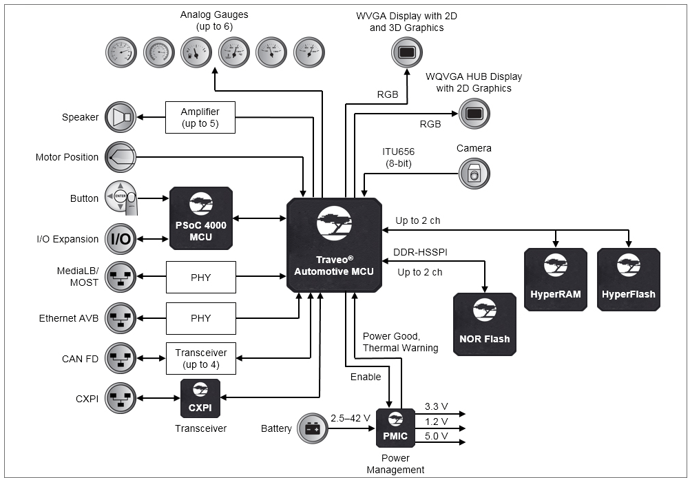
Fig. 7: Instrument cluster system-level diagram. Source: Cypress
Other domains don’t use MCUs. Instead, they incorporate higher-end application processors and SoCs. These devices are used in the various domains, such as the advanced driver assist system (ADAS) and high-end infotainment systems.
These processors don’t integrate embedded flash. Instead, OEMs would use an external NOR device on the board. The processor and NOR device communicate over a bus.
Processors integrate SRAM memory for cache. SRAM stores data and frequently used instructions. SRAM is fast, but it’s large and consumes power.
That’s where embedded STT-MRAM fits in for cache. “With MRAM, because of the fact that the bit cell is much smaller than an SRAM bit cell, you can put a whole lot of MRAM onto the chip,” Objective Analysis’ Handy said.
This would reduce space and cost. “Some people would see MRAM over time as an embedded flash replacement. But that isn’t where we are focused. Where we see it as an opportunity is as a nonvolatile SRAM,” said Ron Martino, vice president of application processors at NXP.
NXP offers an application processor based on a 28nm FD-SOI process from Samsung. Targeted for infotainment systems and instrument clusters, the device incorporates SRAM and other components.

Fig. 8: Another Instrument Cluster Diagram Source: NXP
In the future, the processor will incorporate embedded MRAM. “When combining MRAM with FD-SOI, we see many applications,” Martino said. “It would not be an SRAM replacement. But it would be complementary, where you bring in MRAM to create nonvolatile RAM blocks that are targeted for higher performance. If you can shut down (the system) and retain information, you have ultimate off-state power. If you can combine it with FD-SOI, you can have active states that are very power efficient and you have memory retention states that draw no power. You can create a very compelling solution as power becomes more of an issue.”
But will STT-MRAM ever meet the temperature specs for automotive? “The state of the MRAM technology in the industry is focused first to bring it into manufacturing at lower temperatures. That would be either in the 85 or 105 degrees Celsius temperature ranges. And then, there will be a next phase that brings it up to 125 degrees C,” Martino said. “The first applications that will be benefiting from embedded MRAM are going to be consumer and industrial. And then, you’ll see the use of MRAM over time in automotive.”
To be sure, carmakers are conservative. They won’t move to a new memory type unless it meets spec. In the meantime, OEMs will extend today’s embedded flash as far as possible. Then, when it runs out of steam, the playing field is wide open with several options on the table. Clearly, OEMs must make the right bet in the high-stakes car market.
Related Stories
What’s Next For NOR Flash?
Four Foundries Back MRAM
Etch Techniques for Next-Generation Storage-Class Memory
New Embedded Memories Ahead
 |
 |
 |
|
 |
 |
 |  |
Great article. Thank you for sharing this detailed report.
Interesting and detail insights of NOR and embedded flash marketing analysis. So far standalone with two-chip solution is still the mainstream. Harsh automotive requirements would still limit the device scaling and other emerging memory involved.
Does MRAM now have lower programming current than NOR Flash?