The number of low-density packaging options is increasing as the popularity of advanced packaging grows.

Several packaging houses are developing the next wave of high-density fan-out packages for premium smartphones, but perhaps a bigger battle is brewing in the lower density fan-out arena.
Amkor, ASE, STATS ChipPAC and others sell traditional low-density fan-out packages, although some new and competitive technologies are beginning to appear in the market. Low-density fan-out, or sometimes called standard-density, is one of two main categories in the overall fan-out market. The other type is high-density fan-out.
Generally, fan-out technology provides a small form-factor package with more I/Os than other package types, but it isn’t the only packaging option on the table. Regardless, geared for mobile, IoT and related applications, low- or standard-density fan-out is defined as a package with less than 500 I/Os and greater than 8μm line and space, according to Advanced Semiconductor Engineering (ASE), an outsourced semiconductor assembly and test (OSAT) vendor. Line and space refer to the width of a tiny wire or a metal trace and the space between various traces in a package.
Targeted for mid-range to high-end apps, high-density fan-out has more than 500 I/Os and less than 8μm line/space, according to ASE. TSMC’s InFO technology, the most notable example of high-density fan-out, is incorporated in Apple’s latest iPhones. Other OSATs are chasing after the high-density fan-out market.
The low-density market is also heating up. “InFO-Apple is the dominant one in high-density, but there is also a lot of standard-density (in the market). And there are a lot of devices that can go into this,” said Jan Vardaman, president of TechSearch International.
Among the drivers for standard-density fan-out are audio codecs, power management ICs, radar modules and RF, Vardaman said. And one company—Qualcomm—is the biggest customer in the arena. “It’s more than Qualcomm now,” she said. “We are seeing companies other than Qualcomm move into volumes in this space.”
The market may change in other respects. At last count, several vendors are shipping or readying at least six or more different low-density fan-out technology types. “It depends on how you count them,” said Jérôme Azemar, an analyst at Yole Développement. “In the long-run, there isn’t room for this many architectures, so it is likely that some will disappear or will simply get more and more similar, despite having different names.”

Fig. 1 Companies Offering FO-WLP Source: TechSearch International
Which fan-out technologies will prevail over the long haul comes down to cost, reliability and customer adoption, so chipmakers need to keep a close eye on this business. Here are just some of the main events in the arena:
In total, the overall fan-out market is expected to grow from $244 million in 2014 to $2.5 billion by 2021, according to Yole. Of that, the low-density fan-out market is expected to grow from $350 million in 2017 to $950 million by 2022, according to Yole. “These numbers may be reduced, depending on how many players will switch to fan-out. At the moment, you have a dependency towards some players like Qualcomm. (It also depends on) how fast panel will enter the market and offer a lower cost,” Azemar said.
What is a fan-out?
Fan-out is a relative newcomer on the block. For decades, IC packaging was a straightforward process. “In conventional packaging, the finished wafer is cut up, or diced, into individual chips, which are then bonded and encapsulated,” explained Choon Lee, vice president of advanced packaging at Lam Research.
OSATs continue to use this method, but the big change occurred in the early 2000s when it developed a technology called wafer-level packaging (WLP). “WLP, as its name implies, involves packaging the die while it is still on the wafer,” Lee said in a blog posting. “Because the sides are not coated with WLP, the resulting packaged chip is small in size (roughly the same size as the chip itself), an important consideration in footprint-sensitive devices such as our smartphones. Other advantages include streamlined manufacturing and the ability to test chip functionality before dicing.”

Fig. 2: Traditional vs. WLP packaging flow Source: Lam Research
There are two main types of WLP packages—chip-scale packages (CSP) and fan-out. CSP is sometimes known as fan-in. “Packaging types are mainly driven by the end application,” said Pieter Vandewalle, senior director of marketing at KLA-Tencor. “Fan-in/fan-out WLP are mainly driven by mobile applications, which require high-performing, energy-efficient thin- and small-form-factor packages.”
Fan-in and fan-out are slightly different. One distinction is how the two package types incorporate the redistribution layers (RDLs). RDLs are the copper metal connection lines or traces that electrically connect one part of the package to another. RDLs are measured by line and space, which refer to the width and pitch of a metal trace. As stated above, low-density fan-out is greater than 8μm line/space.
In fan-in, the RDL traces are routed inwards. As a result, fan-in is limited and runs out of steam at about 200 I/Os and 0.6mm profiles.
But in fan-out, the RDL traces can be routed inward and outward, enabling thinner packages with more I/Os. “In fan-out, you expand the available area of the package,” said John Hunt, senior director of engineering at ASE.

Fig. 3: Fan-In to Fan-out Package Source: ASE
In high-density fan-out, Apple is leading the charge. Traditionally, smartphones use package-on-package (PoP) technology for the application processor. In PoP, a memory package is on the top, while an application processor package is on the bottom.
Many smartphone OEMs are sticking with PoP, as the technology is mature and inexpensive. But PoP is running out of steam at thicknesses around 0.8mm. So Apple moved from PoP to fan-out for the application processor in its latest iPhones. Apple’s latest application processor is based on a 10nm process. The chip is housed in TSMC’s InFO fan-out technology, enabling a smaller and thinner package.
In another example, a customer could integrate different devices, such as digital, analog and RF, in a fan-out package. The digital die might be based on an advanced process, while analog and RF use mature technologies.
The dies with advanced and mature processes can be partitioned and then interconnected in the same package. “Fan-out allows you to combine multiple die, either homogeneously or heterogeneously, into an electrical interconnected package,” Hunt said. “We can not only put multiple dies in a package, but we can also put MEMS, filters, crystals and passives into it.”
Fan-out isn’t the only way to incorporate multiple dies into the package. Customers have several options, including 2.5D/3D, fan-out, system-in-package (SiP) and wirebond technology.
Today, 75% to 80% of all IC packages utilize an older interconnect scheme called wire bonding, according to TechSearch. For this, a system called a wire bonder stitches one chip to another chip or substrate using tiny wires.
At the high end, OSATs offer 2.5D/3D, a die stacking technique that uses through-silicon vias (TSVs). Meanwhile, a SiP combines a series of multiple dies and passives to create a standalone function.
What’s the best multi-die packaging technology? It depends on the application. “Whether it’s fan-out or SiP depends on the application, bandwidth requirements and available real estate. Both will offer significant performance improvements from wire-bonded devices,” said Cristina Chu, strategic business development director at TEL NEXX, part of TEL. “Time-to-market is a major advantage for SiP in complex FPGA devices. In some cases, these SiPs can even combine components from different process nodes in the same package.”
Traditional vs. new fan-out
Meanwhile, in the mid-2000s, Freescale and Infineon separately introduced the industry’s first fan-out package types.
In 2006, Freescale introduced a fan-out technology called Redistributed Chip Packaging (RCP). Then, in 2010, Freescale licensed RCP to Nepes. Nepes set up a 300mm line to make RCP technology in Korea. “Nepes is in production for radar and IoT modules,” TechSearch’s Vardaman said. (In 2015, NXP acquired Freescale.)
Originally, Infineon’s eWLB technology was designed for a baseband chip in cellular phones. Infineon still has a 200mm eWLB production line, which is used for radar modules, Vardaman said.
In 2007, Infineon also licensed the eWLB technology to ASE, and a year later, it struck a similar deal with STATS ChipPAC. Later, Infineon licensed eWLB to Nanium, now owned by Amkor. The licensing deals gave these OSATs the rights to make eWLB.
Initially, eWLB was a single-die package, but the technology eventually moved into more complex multi-die configurations with passives.
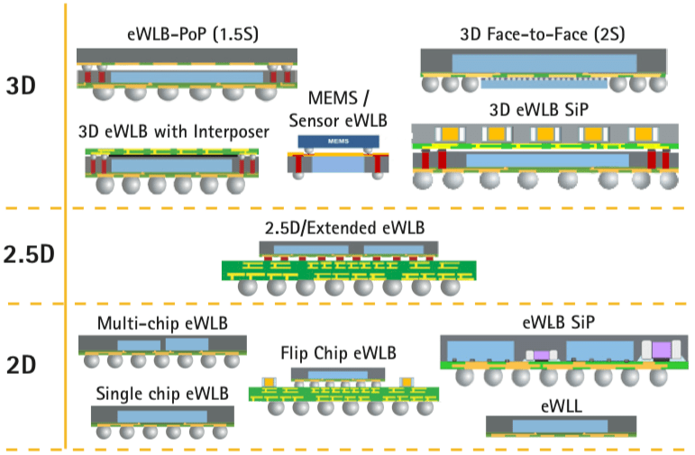
Fig. 4: eWLB product portfolio Source: STATS ChipPAC
“In general, 2D eWLB devices are typical for low- to mid-density applications. The 2.5D and 3D eWLB devices are for high-end or high-performance applications that require more than 500 or 1,000 I/Os. However, there are cases where a 3D eWLB SiP has less than 500 I/Os because of the application requirements,” explained Seung Wook Yoon, director of group technology strategy for the JCET Group. JCET, China’s largest OSAT, in 2015 acquired Singapore’s STATS ChipPAC.
2D eWLB has been shipping since 2009. “We do have a number of 2.5D and 3D eWLB devices that have been qualified by our customers, but they have not reached high-volume production levels yet,” Yoon said.
This package type is manufactured using a chip-first/face-down process flow. Chip-first/face-down is one of three variations of fan-out. The other two include chip-first/face-up and chip-last, sometimes known as RDL first.
In the chip-first/face-down flow, the chips are first processed on a wafer in the fab. Then, the chips are diced. Using a pick-and-place system, the dies are placed on a new wafer based on an epoxy molded compound. This is referred to as a reconstituted wafer.
A reconstituted wafer can be processed in either a 200mm or 300mm round format. The packaging process itself is conducted on this wafer. Then, the dies are cut, forming a chip housed in a fan-out package.
Chip-first has been in production almost a decade. Chip-last, which has a different flow, has not been widely adopted-yet.

Fig. 5: Chip first vs. chip last. Source: TechSearch International
There are some challenges. Reconstituted wafers are prone to warpage in the flow. And when the dies are embedded in a reconstituted wafer, they tend to move during the flow, causing an unwanted effect called die shift. This impacts the yield.
OSATs have overcome many of these challenges. Perhaps a bigger issue occurred in 2016 and 2017, when the two main eWLB packaging suppliers – STATS ChipPAC and Nanium – were sold out of this package type due to demand from Qualcomm.
This, in turn, prompted customers to look for other types of packages, causing a pause in the eWLB market.
In response, STATS ChipPAC and ASE have expanded their eWLB capacities. Then, in 2017, Amkor bought Nanium, a move that provided some backing for the fan-out specialist.
Now, eWLB has three suppliers with sufficient capacity, a move that should jumpstart the market. “There continues to be growing demand for FOWLP in low- to mid-density applications. We have fan-out customers in mobile, 5G or automotive applications that require less than 500 I/Os,” Yoon said. “There are a number of emerging market segments for FOWLP, such as 5G mmWave devices, , fingerprint sensors and automotive applications like advanced driver assistance systems (ADAS).”
In 2018, though, eWLB is expected to get some new competition. ASE, which supplies eWLB, also has been working on another low-density fan-out technology with Deca Technologies. Deca, a subsidiary of Cypress Semiconductor, is the original developer of this technology, dubbed the M-Series.
In addition, ASE is in the process of merging with Siliconware Precision Industries (SPIL), a Taiwan OSAT. SPIL is also working on a fan-out technology called TPI-FO.
Then, in the first half of 2018, ASE plans to move into production with the M-Series fan-out technology. Unlike eWLB, the M-Series is a chip-first, die-up technology.

Fig. 6: M-Series vs. eWLB Source: ASE
The M-Series solves some of the issues with traditional fan-out. “(For traditional fan-out), you have to use a high-accuracy flip-chip bonder to place the die. It’s a relatively low-throughput process. It is around 8,000 dies an hour,” ASE’s Hunt said. “But one of the main problems is die shift. When you place the die after molding, it is not where you placed it. It moves.”
In response, Deca has developed a technology called adaptive patterning. First, the dies are placed on the wafer using a high-speed surface-mount system at a rate of 30,000-35,000 dies per hour. But the placement of each die is less accurate than a traditional system. So to compensate for the accuracy issues, Deca’s technology measures the actual position of every die on the wafer.
“We then recalculate the RDL pattern to accommodate every die shift in every wafer. That recalculation takes about 28 seconds. By the time the wafer gets to the imaging system, the pattern has been recalculated,” Hunt said.
The data then is fed into an imaging system. In eWLB, a traditional lithography system patterns a feature on a die. In contrast, Deca’s technology uses a proprietary laser direct imaging system. Laser direct is like direct-write lithography. It directly writes features on a die without a mask.
In Deca’s technology, the laser direct imaging system aligns the entire RDL pattern to the measured die position, which supposedly solves the die shift problems.
Competitors are keeping an eye on the technology. “Deca M-Series solution has its own unique advantages, but has not yet been proven in high-volume production,” JCET’s Yoon said.
Here comes China
Meanwhile, there are other relative newcomers in fan-out, namely from China. For example, Jiangyin Changdian Advanced Packaging (JCAP) has a wafer-level package. JCAP is part of Jiangsu Changjiang Electronics Technology (JCET). In addition, JCET also acquired STATS ChipPAC.
Tianshui Huatian, another large OSAT in China, develops several package types, including fan-out. “The JCAP one is in production. Huatian is probably close to a production part. The versions in China are different from the original eWLB process,” TechSearch’s Vardaman said.
Tianshui Huatian’s fan-out technology is called eSiFO. In eSiFO, the wafer is etched, forming a gap. Dies are placed in the gaps using a pick-and-place system and then sealed.

Fig. 7: Process Development of eSiFO Source: Tianshui Huatian
“It uses a silicon carrier and does not require a mold compound. It is gaining traction primarily because there is considerably less stress and warpage. There is a minimal CTE mismatch between our silicon carrier wafer and the die embedded inside the dry etched trench. It is also a fundamentally simpler process,” said Allan Calamoneri, vice president of sales and marketing for Huatian Technology Group USA. “Currently, applications are in lower density, smaller packages and recently multi-die configurations. We are in qualification with some U.S. customers, but production volumes are currently only being shipped for China-based customers.”
What’s next? Today’s fan-out packages involve packaging a die in a round 200mm or 300mm wafer format. In R&D, some are working on panel-level fan-out, which involves packaging a die on a large square panel. The idea is to process more dies per unit area, which, in theory, reduces the cost by 20%.

Fig. 8: Comparison of number of die exposed on 300mm wafer to number of die on panel. Source: STATS ChipPAC, Rudolph
ASE-Deca, Nepes, Samsung and others are developing panel-level fan-out. Targeted for 2018 and 2019, panel-level fan-out packages will supposedly enable cheaper, low-density products.
But panel-level packaging is a difficult technology to master, and there are no standards in the arena. “The main parameter of choice is always cost,” Yole’s Azemar said. “The entrance of panel in the equation may change the landscape.”
So which low-density fan-out technologies will prevail over the long run? Some will continue to make inroads. Others may take off or will become niche products. But it’s unclear if there is room for everyone despite the explosion of new apps in the market.
Related Stories
What’s What In Advanced Packaging
Advanced Packaging’s Progress
What Next For OSATs
Betting On Wafer-Level Fan-Outs
Fan-Outs vs. TSVs
Litho Options For Panel Fan-out
Packaging Challenges For 2018
Shortages Hit Packaging Biz
Wirebond Technology Rolls On
 |
 |
 |
|
 |
 |
 |  |
Why do the boosters of latest Adv. Pkg. Technologies e,g. 2.5 d, 3-d die stack, FO WLP, as well as journalists new to the topic try so hard to bury the earlier Flip Chip ( bumping, substrates, die bond ) technology when so many of these later “wafer level ” (!) packaging technologies ( DIE LAST FO WLPs, Amkor SWIFT ) continue to use them ?
How has switching to thinner inFO ( or for that matter other claimed advantages of FO WLPs e,g. lower cost, better electrical performance derived from eliminating the substrate typical of Flip Chip ) benefited iPhones ? Are there compelling arguments for others to switch ?
Would the FO WLP boosters please also try to explain why 2+ years since Apple switched to inFO, no other SoC manufacturer have yet gone the inFO way and QCOMM ( which is a high volume user of FO WLPs for their Codec etc. ) has stayed w/ MCEP ( embedded Flip Chip ) for their flagship APs ?
What happens when a SoC die from a 10 nm Fab with ultra low K ILD for speed is switched from Flip Chip to FO WLP and w/o the benefit of a FC substrate as a stress buffer is subjected directly to board level stresses ?
And as to the boosters hope of pushing high density FO WLPs to replace current expensive 2.5d interposers, what about the heat extraction limits of FO WLPs ? How many ASICs and FPGAs would survive a junction temp of 130 C ?
But best wishes for WLPs to grow within their limits dictated by physics.
Hi. You make some excellent points. Thanks for the feedback. Clearly, the older technologies never die. Flip-chip, QFN and even wire-bond are alive and well. But correct me if I’m wrong, it took flip-chip ages before it gained traction. And you are correct. Flip-chip BGA is the ”go to” package for the apps processor. I’m not sure we are burying that. In a recent blog, I stated that fan-out hasn’t really taken off and is really in the ”disillusionment stage.” https://semiengineering.com/5-takeaways-semicon/ Even so, we need to keep a close eye on fan-out and other new technologies. We need to follow the progress and developments with fan-out–as flip-chip, QFN and wire-bond roll on. So will fan-out ultimately succeed?. Let’s watch it very close.
Hi Mark, great summary. Can you comment on max package size? Most papers cover up to 14 x 14 mm, not large enough for high performance computing.