Challenges persist, but there are enough options available that it won’t limit device scaling.

The replacement of aluminum with copper interconnect wiring, first demonstrated by IBM in 1997, brought the integrated circuit industry substantial improvements in both resistance to electromigration and line conductivity. Copper is both a better and more stable conductor than aluminum. Difficult though the transition was, it helped extend device scaling for another eighteen years (and counting).
But the challenges posed by conductivity and electromigration resistance requirements never really went away. As feature sizes shrink, they are coming to the forefront again. This time, there is no obvious alternative, no metal that is as clearly superior to copper as copper was to aluminum. Instead, the industry faces an ongoing balancing act among what Sree Kesapragada, Applied Materials’ Global Product Manager for metal deposition products, described as the key requirements of any successful interconnect scheme: line resistance, gap fill, and electromigration.
The interconnect balancing act
The resistance challenge is easy to describe, but not so easy to solve. The resistance of a wire increases as the cross-sectional area of the wire gets smaller. Narrower lines have more resistance, dissipate more power, and generate more waste heat. In the case of copper interconnects, two additional factors make the problem worse. One is the relationship between resistivity and line width. The approximate mean free path of electrons in copper is 55nm. As line width approaches that value, sidewall scattering begins to contribute and resistivity climbs dramatically.
Making the problem worse, copper lines are encased in barrier layers to prevent diffusion into the dielectric. If these layers are too thin, they will not perform their function adequately: barrier layer thickness remains relatively constant as line width scales down. The fraction of the line composed of copper shrinks. This, in turn, affects line width-dependent characteristics such as grain structure and resistivity.
The barrier and seed layers also play a key role in gap fill, the second important requirement for an interconnect process scheme. Current generation process schemes typically use sputtered TaN barriers, with a sputtered copper seed layer. Copper wets TaN poorly, though. The combination of poor wetting, vertical sidewalls, and narrow trenches can result in a discontinuous seed layer. Incomplete seed layer coverage can lead to voids and other defects in the copper line, which in turn can weaken adhesion between the copper and the barrier layers. They can also cause poor adhesion between the copper and the barrier layers. Defects and poor adhesion both contribute to electromigration, the third requirement an interconnect process scheme must face.
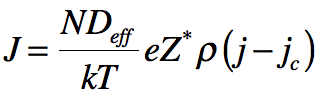
Electromigration, as the name implies, is an atomic flux driven by current through a line. A. S. Oates and M. H. Lin at TSMC modeled the rate of electromigration as a function of current density and diffusion rate:
where J is the net flux of atoms, N is the atom density, ![]() is the effective diffusivity, eZ* is the effective charge, ρ is resistivity, and kT is Boltzmann’s constant times temperature. The effective current density,
is the effective diffusivity, eZ* is the effective charge, ρ is resistivity, and kT is Boltzmann’s constant times temperature. The effective current density, ![]() is modified by the Blech effect, discussed below.
is modified by the Blech effect, discussed below.
Narrow lines, more migration pathways
Current density increases as lines become narrower. The critical current density at which migration occurs can vary, depending on the morphology, nucleation rate, and growth rate of voids in the material. Likewise, the diffusion rate depends on the microstructure of the material. In aluminum, very little electromigration occurred at grain boundaries, and so migration was largely independent of microstructure.
With copper interconnects, however, there are three possible migration pathways: along grain boundaries; along the top surface, between the copper line and the dielectric top barrier layer; and along the trench sidewalls, between the copper line and the metal barrier layer. This last pathway generally can be neglected in current generation devices because metal-to-metal adhesion is typically strong. However, as new, thinner barrier layer materials are introduced to increase the copper cross-section, they can bring adhesion and electromigration concerns with them.
So far, typically the most important electromigration pathway has been along the top surface, as adhesion between the dielectric barrier and the copper is typically weak. Since about the 28 nm node, Kesapragada explained, manufacturers have doped copper seed layers with manganese. Manganese diffuses to the surface, improving top barrier adhesion and helping to impede migration. In smaller lines, however, the confined structure leads to smaller grains. Manganese becomes trapped at the grain boundaries and does not reach the top surface. On the other hand, as Cathryn Christiansen and coworkers at IBM showed, manganese incorporated at the grain boundaries can help slow migration along that pathway.
The polycrystalline structure of very narrow copper lines also introduces another electromigration pathway. The activation energy for void formation is lower at grain boundaries than in the bulk. Once voids nucleate, copper can migrate through them. (This is another reason why void-free gap fill is important, too.) Oates and Lin found that grain boundary diffusion increases with the polycrystalline fraction (p) of the film. Interface electromigration is dominant for p < 0.7, but they saw an order of magnitude increase in average drift velocity for 0.9 > p > 0.7. While in theory, larger grains could reduce electromigration, controlling grain size in nanometer-scale features is extremely difficult. Some processes do use a post-deposition anneal to encourage grain growth, but the benefits of more aggressive measures like grain boundary dopants or attempts to control grain orientation are not clear.
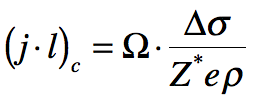
Some good news: the Blech effect
Working in opposition to electromigration is the Blech effect: migration creates tensile stress at the upstream, cathode, end of the line, and compressive stress at the downstream, anode end. The sidewalls, being rigid, supply back pressure against this stress, slowing migration. The Blech effect is line length dependent: shorter lines offer more resistance. S. Thrasher and colleagues at Motorola found that there is a critical value of the length-current density product below which no migration occurs:
where Ω is the atomic volume and Δσ is the stress gradient.
This has led to electromigration-driven design rules, limiting the allowable wire length as a function of current density. It is not always clear, however, just where line segments begin and end for the purpose of evaluating electromigration risk, and it is not always easy to quantify the benefits that the Blech effect can provide.
Researchers at IBM conducted an extensive analysis to determine the best ways to define the length of non-trivial line segments, and to evaluate the results.
The difficulty in balancing resistance, gap fill and electromigration becomes especially clear when considering proposals for alternative barrier and seed layers. Thinner barrier layers are desirable because they increase the portion of the total line width available for copper. However, in addition to the risk that a thinner diffusion barrier will be less effective, thinner layers are generally less rigid. A thinner layer might reduce or eliminate the Blech effect back pressure against electromigration, which the designer may be depending on to keep reliability within specifications. Here, paradoxically, longer lines actually have an advantage over shorter lines. Longer lines do not benefit from the Blech effect, and therefore their performance does not suffer if it is reduced. An alternative barrier might also have weaker copper adhesion, increasing the potential for migration along trench sidewalls.
Will the process save us?
An extreme example of the second issue is provided by ruthenium, which has been proposed as an alternative seed layer. Copper flows freely enough along ruthenium surface to be used in a “reflow” deposition scheme: rather than depending on the plating chemistry alone to maintain bottom-up filling of copper lines, copper flows downward along the ruthenium sidewalls, creating an even, void-free fill.
Unfortunately, these same flow characteristics tend to suggest that electromigration along the copper/barrier interface could be a problem for ruthenium reflow processes. At the 2014 IEEE Electron Device Meeting (IEDM), researchers at Samsung described a ruthenium integration scheme with migration characteristics comparable to those achieved by other processes. To this date, however, as Kesapragada observed, there are no reports of successful ruthenium integration in production devices.
To this point, selective CVD of cobalt cap layers appears to be the most promising alternative scheme. Selective deposition allows the use of a metallic, rather than dielectric, top barrier surface, improving both conductivity and adhesion. Cobalt also serves as an adhesion promoter to facilitate adhesion of the copper seed layer. CVD liners are conformal, making it possible to achieve a uniform coating in a thinner layer than with sputtering alone. Cobalt does not appear to impede grain boundary migration, which as noted above is likely to become the dominant pathway in future technology nodes. However, it may be possible to combine a cobalt liner and cap layer with a manganese-doped copper seed layer, gaining the benefits of both technologies.
The consensus of the industry appears to be that electromigration challenges are manageable through a combination of current density-based design rules and process enhancements to improve copper adhesion. Resistance is likely to impose more severe constraints on interconnect schemes, particularly as line width approaches the mean free path of electrons in copper. For overall reliability, as TSMC’s Anthony Oates explained at the 2014 IEDM, gate dielectrics and charge trapping in the gate stack are perhaps the most serious concern, and will be addressed in a future article. http://ieeexplore.ieee.org/xpl/articleDetails.jsp?tp=&arnumber=7047092

 |
 |
 |
|
 |
 |
 |  |
Katherine
Your history is way off. As is your analysis of Al electromigration. The part you got right is the bit about how we can design around it.
Care to elaborate? I fact checked reasonably carefully.
Did anyone study the effects of moisture or the lack of (N2 only) related to electromigration
In what context? Wires inside the IC itself (as opposed to the package) aren’t generally exposed to much moisture.
You are quite right here.
Jorgen
I feel you are not thinking of electromigration. It is due to momentum exchange between diffusing metal atoms and conducting electrons and moisture does not come into play. Some papers erroneously call any field assisted diffusion electromigration and that’s probably where tour confusion is.
The Blech length work goes way back to the 1970s. I also seem to remember in the article you said that grain boundary diffusion in Al didn’t happen, in fact that was where all the mass transport was occurring. Later in when they got bamboo structure Al, there could be some justification for that statement, but bamboo structure was never perfect, we had bamboo like films, but there were long grain clusters that made the use impossible. Electromigration goes back over 50 years and has a fascinating history. I would like too continue, but I need to go now.
Yes, the Blech effect was first described in 1976 by I. A. Blech, who studied aluminum lines. J. Appl. Phys., 47, 1203 (1976). Since this was written as a news article, not a historical or technical review, I only referenced the papers directly relevant to my point, in this case the Thrasher SPIE paper from 2000.
My source for the relationship between microstructure and electromigration in aluminum was Lin and Oates, IEEE Trans. Dev. and Mater. Rel., 11, 540 (2011). Yes, they were referring to bamboo microstructure, since that had in fact been achieved by the time copper was introduced.