New lithography tools will be required at 5nm, but pellicles, resists and uptime are still problematic.

Momentum is building for extreme ultraviolet (EUV) lithography, but there are still some major challenges to solve before this long-overdue technology can be used for mass production.
EUV lithography—a next-generation technology that patterns tiny features on a chip—was supposed to move into production around 2012. But over the years, EUV has encountered several delays, pushing out the technology from one node to the next.
As it stands today, GlobalFoundries, Intel, Samsung and TSMC are racing each other to insert EUV lithography into high-volume manufacturing (HVM) at 7nm and/or 5nm, which spans from the 2018 to the 2020 timeframe, depending on the vendor. Additionally, Micron, Samsung and SK Hynix hope to use EUV for 1xnm DRAMs.
But as before, there are several pieces that must come together before EUV moves into HVM. And chipmakers must also weigh an assortment of complex tradeoffs.
Based on the latest data from the industry, here is a snapshot of the status of EUV today and some of those tradeoffs:
• ASML is installing its first production-worthy EUV scanner with its long-awaited 250 watt power source, which is due out by year’s end. Uptime for EUV remains an issue, however.
• Resists, the materials that form patterns on a surface when exposed to light, are struggling to meet the targeted spec for EUV today. The spec can be reduced, but throughput takes a hit. And at times, the interactions with the resists can cause variations in the process and even pattern failures.
• EUV pellicles, a key part of the mask infrastructure, are not ready for HVM. Pellicles are thin membranes that prevent particles from landing on the mask. So chipmakers may either wait for the EUV pellicles or move into production without them, at least initially.
Still, even without some of these pieces in place, chipmakers could insert EUV lithography at 7nm. Using a brute-force approach, EUV could be inserted for a layer or so. At 5nm and beyond, though, EUV isn’t ready to meet the tighter specs at these nodes, meaning the industry must spend more time and money to work out the problems.
“We are getting closer to having EUV at high-volume manufacturing implementation,” said Patrick Ho, an analyst at Stifel Nicolaus. “A few things need to be resolved and customers do vary on how many layers they will utilize for EUV. Intel is more conservative. Samsung is more bullish, as they want to get it into both DRAM and foundry/logic. I believe full HVM implementation will occur at the TSMC 5nm node, which time-wise likely means 2020-2021.”
Clearly, foundry customers need to stay ahead of the curve for EUV. To help the industry gain some insights, Semiconductor Engineering has taken a look at the technology and some of the trade-offs for the three main parts of EUV—scanner/source; resists; and mask infrastructure.
Why EUV?
Today, chipmakers use 193nm wavelength lithography to pattern the fine features on a wafer. In reality, though, 193nm immersion lithography hits the limit at 80nm pitch (40nm half-pitch).
So starting at 22nm/20nm, chipmakers began to use 193nm immersion lithography along with various multiple patterning techniques. Aimed at reducing the pitch beyond 40nm, multiple patterning involves a process of using several lithography, etch and deposition steps in the fab.
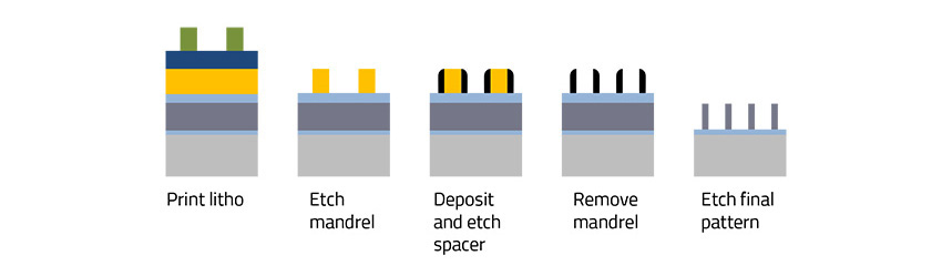
Fig. 1: Self-aligned spacer avoids mask misalignment. Source: Lam Research
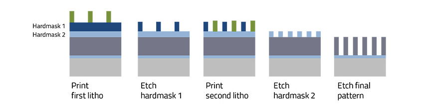
Fig. 2: Double patterning increases density. Source: Lam Research
Multiple patterning works, but it adds more steps, thereby increasing the cost and cycle time in the flow. Cycle time is the amount of time it takes to process a wafer in a fab from start to finish.
To address these issues, chipmakers want EUV. But because EUV is not ready for the initial stages at 7nm, chipmakers will first use immersion/multi-patterning. The hope is to insert EUV later at 7nm. EUV is a must for 5nm.
“7nm will be made practical with optical, though probably not ideal from a cost perspective,” said Aki Fujimura, chief executive of D2S. “(The industry is) hoping to have EUV for the same design rules later as the volume ramps up for 7nm. 5nm is really not attainable from a practical standpoint without EUV.”
Initially, EUV is targeted for contacts and vias at 7nm. To process contacts/vias, it requires two to four masks per layer for optical lithography at 7nm, according to GlobalFoundries.
With EUV, though, it requires only one mask per layer to process contacts/vias at both 7nm and 5nm. In theory, EUV simplifies the flow and reduces the cycle time by about 30 days in the fab, according to ASML.
“That’s a pretty good tradeoff because you’re trading quad patterning or triple patterning of the contacts for one mask,” said Gary Patton, chief technology officer at GlobalFoundries. “That doesn’t affect any of the design rules either, so the customer can get the advantage of that in cycle time and better yield. And as it is ready, we’ll transition (EUV) over to where we’ll do metal levels and shrinks.”
So, EUV is doable at 7nm, arguably even with single patterning. At 5nm, though, the specs are tighter and feature sizes become smaller. For this, chipmakers may require EUV with multiple patterning, a complex and expensive process at best.
The early adopters for EUV hope to insert the technology for 7nm around 2019 to 2020. “That’s kind of the center. We are trying to be more aggressive,” said Harry Levinson, senior fellow and senior director of technology research at GlobalFoundries. “The four major chip companies are all on a trajectory for HVM over the next couple of years. Now, the real question is who is going to be first and who will be second.”
Source of the problem
Before all that happens, however, chipmakers must first bring EUV into HVM. This has proven to be more difficult than previously thought as the complexity of EUV lithography is mind-boggling.

Fig. 3: The complexity of EUV. Source: ASML
In EUV, a power source converts plasma into light at 13.5nm wavelengths. Then, the light bounces off a complex scheme of 10 multi-layer mirrors.
At that point, the light goes through a programmable illuminator and hits the mask. From there, it bounces off six more multi-layer mirrors and hits the wafer at an angle of 6%.

Fig. 4: Accurately bouncing light. Source: ASML/Carl Zeiss SMT Gmbh.
The big challenge is the power source. It doesn’t generate enough power or EUV light to enable an EUV scanner to go fast enough or make it economically feasible.
To put EUV into HVM, chipmakers want an EUV scanner that can generate 250 watts of power. This translates to a throughput of 125 wafers an hour (wph).
Achieving those targets has taken more time than expected. Not long ago, the source generated only 10 watts of power. Then, ASML’s power source moved from 80 watts to 125 watts, boosting the throughputs for EUV from 60 wph to 85 wph.
Today, ASML is readying its first production EUV scanner, the NXE:3400B. The tool has a numerical aperture of 0.33 and a 13nm resolution. “If you look at the imaging performance of the system, we have (accomplished) 13nm LS and 16nm IS,” said Roderik van Es, senior product manager at ASML. (LS refers to line and space, while IS is isolated lines.)
Initially, the tool will ship with a 140-watt source, enabling a throughput of 100 wph. Recently, ASML has demonstrated a 250-watt source. An industrialized version of the 250-watt source will ship by year’s end, according to Es.
Even with a 250-watt source, though, lithographers are worried about the uptime of the system. Today’s 193nm scanners can run non-stop in the fab at 250 wph or faster. In comparison, the uptimes with the pre-production EUV machines are hovering around 70% and 80%.
“Availability, or how long a tool can run before it needs to be taken down for maintenance, remains a bit of a concern, particularly for Intel,” Stifel Nicolaus’ Ho said. “There cannot be availability levels of 70% or even 80% for companies like Intel that want a high 90s availability metric.”
Still to be seen, however, is how well the NXE:3400B will perform in the field. If there are still uptime issues, lithographers are mulling the idea of buying extra tools for redundancy purposes.
That, of course, is an expensive proposition chipmakers would prefer to avoid. Each EUV scanner sells for roughly $125 million, compared to $70 million for today’s 193nm immersion scanners, analysts said.
Resist issues
For years, the number one challenge with EUV was the power source. Now the top challenge is shifting from the source to the processes involving the resists.
EUV resists fall into two main categories—chemically amplified resists (CAR) and metal-oxide. Used in the industry for years, CAR makes use of a diffusion-based process. The newer metal-oxide resists are based on a tin-oxide compound.
Resists also involve a tradeoff between three metrics in the so-called RLS triangle—resolution (R), line-edge roughness (LER) and sensitivity (S).
To reach the desired resolution, chipmakers want EUV resists at a sensitivity or dose at 20mJ/cm². These resists are available, but they are more difficult to put into HVM than previously thought.
“At 32nm pitch and below, nothing works—neither CAR or metal-oxide regardless of dose, at least within reason (<100mJ/cm²),” GlobalFoundries’ Levinson said.
The industry, however, has developed EUV resists that work at 30mJ/cm² and 40mJ/cm². Based on the principles of the RLS triangle, the higher dose resists provide better resolution. But they are slower and impact the throughput of EUV.
With a 30mJ/cm² dose, an EUV scanner with a 250-watt source has a throughput of about 104-105 wph without a pellicle, according to ASML, which is below the desired 125 wph target.
“Existing EUV resists are capable of supporting 7nm HVM, but we fall off a cliff as we go to smaller CDs,” Levinson said. “The next node may be at risk because too much time was lost pursuing low dose resists.”
This is in reference to the time and money spent to develop resists at 20mJ/cm². The industry is working on these resists, which are targeted for 5nm.
The resist challenges are daunting. “The dose is not necessarily where we would like it to be,” said Richard Wise, technical managing director at LAM Research, at a recent event. “There are a lot of fundamental physical challenges to lower that dose because of the stochastic effects in EUV.”
Stochastics is another way of saying random variations. “Light is made of photons. The number of photons that expose a small volume of resist has an average value corresponding to the desired exposure dose,” explained Chris Mack, chief technology officer at Fractilia. “But there is a random variation about this average. If the number of photons exposing that volume of resist is high, the relative random variation is small. But as the number of photons exposing some small volume of resist becomes smaller, the relative variation in that number becomes large.”
This effect is called photon shot noise. Shot noise is the variation of the number of photons in a lithographic process.
All types of lithography suffer from stochastics, but it is worse for EUV. “First, EUV photons carry 14 times more energy than 193nm photons. So for the same exposure dose, there are 14 times fewer photons,” Mack said. “Second, we are trying to get the throughput of our EUV scanners higher by using a low exposure dose. This means fewer photons, as well. With fewer photons, there is a great random uncertainty in photons or shot noise.”
Variations in the number of photons are problematic. “We have higher-energy photons, but not enough of them. So we have line-width roughness and line-edge roughness (in the patterns),” said Ben Rathsack, senior member of the technical staff at TEL. (LER is defined as a deviation of a feature edge from an ideal shape.)
If that isn’t enough, variations can also cause other issues. “What we would describe as challenge number one in imaging is in the extreme roughness events or the stochastic failures in places like nano-bridging, line breaking and merging or missing holes,” said Gregory McIntyre, director of the Advanced Patterning Department at Imec.
So in the EUV exposure process, the scanner can sometimes fail to resolve a line, space or a contact. Or the process can cause the lines to break or the contacts to merge.
Pellicle problems
Besides resists, there are other issues, namely the EUV photomask infrastructure. The photomask is a master template for a given IC design. After a mask is developed, it is shipped to the fab. The mask is placed in a lithography tool. The tool projects light through the mask, which in turn patterns the images on a wafer.
For years, the industry has been making EUV masks, although the process is still challenging. “The mask sector is ramping up efforts on development of EUV reticles,” said Weston Sousa, general manager of the Reticle Products Division at KLA-Tencor. “The challenges are numerous, from blank quality and CD uniformity, to pattern defectivity and repair.”
Cost and yield are also issues. “It’s the masks that I’m worried about,” GlobalFoundries’ Patton said. “There are both defects in the mask itself and defects that come onto the mask when it’s in manufacturing.”
Data from a recent eBeam Initiative survey showed that overall mask yields are at a healthy 94.8%, but EUV mask yields are down around 64.3%.
And at each node, mask defects become smaller and harder to find. “Defect criteria are looser during the early cycle. It will progress over time to an HVM level. The HVM levels are certainly not loose,” said Jeff Farnsworth, director of mask technology for Intel Mask Operation, the captive photomask unit of Intel.
Moreover, an EUV mask is up to eight times more expensive than a complex optical mask, according to Heebom Kim, a researcher from Samsung. But as EUV moves into HVM, EUV mask costs will likely fall to less than three times more expensive than optical, according to ASML.
Optical and EUV masks are different. In optical, a mask blank consists of an opaque layer of chrome on a glass substrate.
In comparison, an EUV mask blank consists of 40 to 50 alternating layers of silicon and molybdenum on a substrate. In both optical and EUV, the mask blank is patterned, creating a photomask.
Mask makers hope to achieve two goals. The first is to produce defect-free EUV masks. Then, they hope to prevent defects from landing on the mask. In this case, particles from the scanner or other processes can inadvertently fall on a mask.
If defects are present on the mask in the EUV scanner during the exposure phase, they may print on the wafer, thereby impacting chip yield.
Generally, mask makers are making strides in producing defect-free masks. Preventing particles from landing on the mask is a different matter and involves a key piece in the mask infrastructure—the pellicle. A pellicle serves as a dust cover for the mask.

Fig. 5: Prototype pellicle. Source: ASML
Not long ago, the industry insisted that an EUV scanner could process wafers in a clean environment without a pellicle. Chipmakers then changed their position, saying there is no guarantee that the EUV scanner or other tools can remain 100% clean during the flow. Without a pellicle chipmakers say the EUV mask is prone to particles and defects.
So the industry began to develop EUV pellicles. A pellicle for an optical mask is based on a thin polymer material. In contrast, ASML, the sole supplier of EUV pellicles, has developed a polysilicon-based EUV pellicle that is just 50nm thick.
In operation, when EUV light hits the pellicle, the temperature of the membrane will heat up anywhere from 600 to 1,000 degrees Celsius.
The problem is that the pellicle is brittle. At those temperatures, some fear that the EUV pellicle could deteriorate during processing, causing damage to the EUV mask and scanner.
So far, ASML’s EUV pellicle has been tested with an EUV power source at 140 watts. But it’s still unclear how the pellicle will react to a 250 watt source.
“For the mechanical strength and application properties, EUV pellicles have some challenges,” said Banqiu Wu, principal member of the technical staff and CTO of the Mask and TSV Etch Division at Applied Materials. “The pellicle absorbs some EUV energy. This energy will cause the pellicle temperature to increase. The pellicle also resides in a vacuum. That means natural convection cooling is very low. The natural heat transfer is very difficult, because the pellicle is so thin.”
All told, there is still some uncertainty, if not skepticism, about the use of polysilicon-based pellicles in HVM. So now, the industry is changing its tune and considering two options—wait for an HVM pellicle or start production without them.
Intel, for one, has stated it would not move into EUV production without a pellicle. “We are aggressively pursuing it,” Intel’s Farnsworth said.
The industry is hedging its bets, however. Many also are considering a plan to move into EUV production without the pellicle, at least initially.
In theory, with EUV, chipmakers could process contacts and vias without a pellicle. “There’s no need for a pellicle for those, because the critical area is smaller. So the risk of a particle creating a problem is less,” GlobalFoundries’ Patton said.
There are some consequences, however. Unwanted particles are bound to land on the mask even if the EUV scanner is clean.
So if chipmakers move into production without a pellicle, they must implement more mask inspection and cleaning steps in the flow. “We will do what we have to do with wafer print and wafer inspection,” GlobalFoundries’ Levinson said. “But it’s painful. So, we need a good pellicle solution.”
In R&D, the industry is working on next-generation pellicles and other parts of the mask infrastructure. To be sure, there is also a sense of urgency regarding the development of EUV resists. And, of course, there is the power source.
Will it all come together? Time will tell in the ongoing saga of EUV lithography.
—Ed Sperling contributed to this report.
Related Stories
Why EUV Is So Difficult
Unsolved Litho Issues At 7nm
Challenges Mount For Photomasks
Survey: Optimism Grows for EUV
 |
 |
 |
|
 |
 |
 |  |
As I had mentioned in the other article on 7nm Litho Issues, the different aberrations at different slit positions would mean multiple patterning (i.e., multiple masks) where one layer is divided into stripes corresponding to each (differently SMO-corrected) slit position.
https://nikonereview.com/2017/mentor-graphics-director-details-challenges-for-edge-placement-control-in-2020/
Hi memister. Good points. Thanks. Let’s also see if EUV can meet the EPE targets. EPE is also key. https://semiengineering.com/patterning-problems-pile-up/
Can anyone tell me is it not possible for Intel, Samsung or Glofo to adopt Canon Nil tech instead of Euv?
Hi Sarit. My opinion: NIL is not possible for 7nm/5nm logic, at least today. NIL defects are too high. Overlay is not good enough. Some day, however, I would like to see NIL compete with EUV in logic…..However, NIL is a good candidate for NAND flash. NIL might be used to pattern the holes/channels for 3D NAND. I might be wrong. Any other thoughts out there (Canon or DNP)?
Thanks a lot for the answer Mark, I am just a typical pc user that fascinated with the chip design and technology, The more i read into it the more i am amaze with what the people in the industry have done to get us this far.