Panels could sharply reduce the cost of fan-outs, but this approach will require new equipment.

Several packaging houses are inching closer to production of panel-level fan-out packaging, a next-generation technology that promises to reduce the cost of today’s fan-out packages.
In fact, ASE, Nepes, Samsung and others already have installed the equipment in their panel-level fan-out lines with production slated for 2018 or so. But behind the scenes, panel-level packaging houses continue to evaluate the equipment vendor base, particularly in lithography, according to multiple sources. Lithography is the key technology that creates or patterns the critical features in IC packages as well as chips in the wafer fab.
Besides the vendor base, sources say that packaging houses are also taking a hard look at the three main lithography tool types for panel-level fan-out—excimer laser ablation, laser direct imaging and steppers. Most panel-level packaging houses will use traditional steppers, although some will opt for laser-direct imaging, a maskless lithography technology. Ablation, a removal process, also is being evaluated.
Packaging vendors are exploring the lithographic landscape, and for good reason—panel-level packaging presents some new and major challenges in the industry. It may even require some new breakthroughs and approaches to produce cost-effective panel-level packages with good yields.
Today’s fan-out packages involve packaging a die in a round 200mm or 300mm wafer format. In R&D for some time, panel-level fan-out involves packaging a die on a large square panel. The idea is to process more dies per unit area as a means to reduce the cost of fan-out packaging.

Fig. 1: Comparison of number of die exposed on 300mm wafer to number of die on panel. Source: STATS ChipPAC, Rudolph
But panel-level packaging is a difficult technology to master, and there are no standards in the arena. Several vendors are working on different panel sizes. And then, it will take time before the market reaches critical mass. “You are not going to see volumes until the end of 2018 or in 2019,” said Jan Vardaman, president of TechSearch International.
The return-on-investment is also cloudy. For one thing, it requires $100 million to set up a new panel-level packaging line, said Vinayak Pandey, vice president of product and technology marketing at STATS ChipPAC, in a recent presentation.
“The second big thing is finding a sweet spot from a customer perspective (for panel-level fan-out). A lot of customers are still in the flip-chip space, with the exception of one,” Pandey said, referring to a competitive packaging interconnect scheme called flip-chip. “When we look at 10nm designs, flip-chip meets their requirements. You can go to fan-out, but we see that flip-chip can meet the requirements. So we are hoping that when we get to 7nm or maybe sub-7nm, there are applications (for panel) that can drive value for the customer.”
Clearly, there are several dynamics at play with panel-level packaging. To help customers get ahead of the curve, Semiconductor Engineering has taken a look at the panel-level fan-out market and the various lithography options in the arena, such as ablation, direct imaging and steppers.
Why panels?
Fan-out packaging is hot. In total, the overall fan-out packaging market is expected to grow from $244 million in 2014 to $2.5 billion by 2021, according to Yole Développement. “While panel fan-out is almost nothing in terms of revenues in 2017, we expect it to reach around 15% of overall fan-out production in 2022, reaching a packaging market size of $253 million,” said Jérôme Azémar, an analyst with Yole.
Apple, Qualcomm, NXP and others are developing chips using today’s wafer-level fan-out packages. This is evident in the smartphone world, where package-on-package (PoP) technology traditionally was used for the application processor. Typically based on flip-chip, PoP is inexpensive and reliable, but the technology is running out of steam in terms of I/Os and package thickness. So Apple moved from PoP to TSMC’s InFO fan-out technology for the latest iPhones to provide a smaller package with more I/Os.
Besides TSMC, other packaging houses have introduced fan-out packages based on the various flavors of the technology, such as chip-first and chip-last.
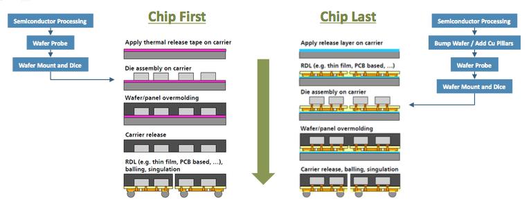
Fig. 2: Chip first vs. chip last. Source: TechSearch International
In today’s wafer-level fan-out packaging flow, individual dies are embedded in an epoxy material in a 200mm or 300mm round wafer. The dies are processed and diced, resulting in single- or multi-die fan-out packages.
In fan-out, the interconnects are fanned out, enabling more I/Os. It also doesn’t require an interposer, making it less expensive than 2.5D/3D devices with through-silicon vias (TSVs).
But fan-out also has some cost issues. “Wafer-level fan-out packaging can represent a substantially lower price point compared to TSV, but it is still cost prohibitive for many products, especially for multi-chip packages that are typically greater than 20mm in size,” according to Jon Hander, director of advanced technology from TEL NEXX, and Cristina Chu, strategic business development director at TEL NEXX. TEL NEXX, part of TEL, is a supplier of electrochemical deposition (ECD) tools.
So fan-out is not an option for many customers. Instead, they will continue to use the more traditional and inexpensive packaging types, such as fan-in, flip-chip and wirebond. “From what we see in our customer base today, WLFO is already in the works or on their development roadmaps. However, as with any business, there needs to be a competitive or technical benefit over the existing packaging options. Today, there are still a number of devices that have been optimized for wirebond or flip-chip. As we saw with WLCSP, the end applications and their success will drive how quickly WLFO will prove what analysts have projected in the coming years in terms of its growth,” said Gil Chiu, regional vice president of North America at Unisem, a packaging house.
That’s the idea behind panel-level packaging. By increasing the substrate size, a vendor processes more dies as a means to lower the cost. A 500mm x 500mm panel, for example, can process 4.54 times as many die as a 300mm wafer, according to a paper from STATS ChipPAC and Rudolph Technologies.
“510mm x 515mm panel substrates could deliver a greater than three-fold increase in substrate area for less than a 50% increase in cost,” according to TEL NEXX’ Hander and Chu. “The cost reduction is compelling for a transition from 300mm wafer to 510mm x 515mm panel, but meeting the technology requirements now and in the future for high yielding panel-level fan-out must be proven.”
Indeed, panel-level fan-out has many of the same challenges as today’s wafer-level fan-out. “For wafer handling, the reconstituted wafers used in FO-WLP can exhibit significant warpage, and maintaining feature dimensions across wafer topography becomes challenging,” said Justin Oberst, a process engineer at Lam Research, in a recent presentation. Lam supplies ECD tools for packaging.
Panel-level processing is conducted at a much larger scale, so warpage and uniformities become even more problematic. On top of that, there are no standards. Today, more than a half-dozen companies are working on panel-level packaging with different panel sizes.
Despite the challenges and lack of standards, ASE, Nepes, Samsung as well as several R&D organizations are readying their panel-level fan-out lines with production slated over the next year.
Others are still evaluating the technology, while still others are not pursuing it. For example, TSMC has been successful with wafer-level fan-out and insists it doesn’t require a panel.
Then, Intel has been developing a generic panel-level packaging technology based on a 510mm x 515mm format. Intel has not entered the fan-out market—yet.
“Panel is happening, but it’s not for what you would call integrated fine-pitch packaging,” said Markus Arendt, president of Suss Microtec’s Photonic Systems unit. “Also, we don’t see a lot of OSATs that will engage in this. The problem for OSATs is that some of the products that they package (are in markets where) the volumes are so small. That could probably populate one panel to fill the entire production needs for a customer for a year.”
Arendt added that companies moving into panel-level packaging already have panel experience. Both Intel and Samsung have panel experience.
Regardless, panel-level packaging requires a different set of equipment. “It’s not simply the processing equipment,” said John Hunt, senior director of engineering at Advanced Semiconductor Engineering (ASE), in a recent interview. “You have to put the whole infrastructure together with a panel process.”
Litho choices—the stepper
In packaging, there are many process steps. Lithography, arguably the most critical process, is used to create various structures in packages, such as bumps, copper pillars, RDLs and TSVs.
The redistribution layers (RDLs) are among the most critical structures in packages. RDLs are the copper metal interconnection schemes or metal traces that route the electrical signals from one part of the package to another.

Fig. 3: Redistribution layers. Source: Lam Research
RDLs are measured in terms of line and space, which refers to the width of the metal traces and the space between them.
There are several ways to fabricate the RDLs. A seed layer is deposited or sputtered on the surface. A resist is applied and then exposed using a lithography system. Copper is deposited using ECD.

Fig. 4: A common RDL flow. Source: Chipbond
Today’s wafer-level fan-out packages range from 5µm line and space (5-5µm) and above with 2-2µm and beyond in R&D. For panel-level fan-out, though, packaging houses will likely start out at 10-10µm. Over time, they will move to 5-5µm and beyond.
To pattern the RDL layers, packaging houses use two types of optical-based lithography systems—mask aligners and steppers. Mask aligners, which are used to process features at 3-3μm and above, might play a role in panel.
For panel-level packaging, the stepper appears to be the favorite option. For years, steppers have been used for fine-pitch applications in wafer-level fan-out and other package types.
“Steppers continue to be the preferred choice due to their capability to provide fine feature performance, high throughput and reliability,” said Rezwan Lateef, vice president and general manager for lithography products at Ultratech.
With steppers, the process is straightforward. A chip layout is transformed from a file format into a photomask. The mask, a template of a given layout, is placed in the stepper.
The stepper projects light through a lens and the mask, forming an image on a small portion of the wafer. The substrate is then moved and imaged again. This process is repeated.
For packaging, some steppers are configured with a broadband light source that enables three different wavelengths—g, h and i (436nm, 405nm and 365nm). A “ghi” stepper is used for applications at 2-2μm and above.
Other steppers are i-line only. With a 365nm wavelength, i-line steppers are used for more advanced packages beyond 2-2μm.
Then, some steppers process a feature at a scale of 1:1 or 1X. Meanwhile, reduction steppers image a feature at 2X, 4X or 5X.
So what’s the right solution for panel-level packaging? “With regards to i-line versus ghi-line, since the line/space requirements are typically well above 2µm (for panel-level fan-out), either mode can be utilized,” Lateef said.
The real issue is that lithography suppliers simply can’t take an existing system for wafer-level packaging and sell it into the panel market. Instead, lithography vendors must more or less build a new tool or revamp one for panel.
“Since we are talking about substrates that are much larger than a 300mm wafer, the whole system has to scale up, which includes the technically complex wafer stage utilized for the exposure process,” he said. “This stage then also has to handle the warpage issues. The handler is probably less problematic as there are vendors who are capable of handling panels.”
Some vendors already have developed lithography and other tools for panels. But panels present a dilemma for toolmakers that haven’t committed to the technology. It costs time and money to build a new tool, yet it’s unclear if or when panels will take off.
If that is not enough, processing a panel-level substrate has its own set of challenges. “There are still a variety of lithography requirements that vary depending on the manufacturer,” he said. “For instance, a recent survey of panel-level packaging manufacturers revealed that panel sizes can vary from 370mm x 470mm to 600mm x 600mm, which can correlate to substantial process variation.”
In addition, a lithographic tool must have the ability to pattern features in thicker films. Thicker films are prone to topographical variations in the process.
Another issue is called die shift. In fan-out, dies are embedded in a reconstituted wafer. But at times, the dies move during the flow, causing the dies to shift. “In our view, the biggest challenges are in the metrology and correction of die placement and shift,” said Rich Rogoff, vice president and general manager of the Lithography Systems group at Rudolph Technologies. “Warpage of material, sometimes exceeding 10mm, and throughput are also a challenge.”
Rudolph and STATS ChipPAC recently presented a paper that solves the die shift issues in panel processes. Using Rudolph’s stepper, the companies used an older technique called “mapping.”
Mapping uses an algorithm to measure the actual die placement position in relation to its desired location. The data is processed by the stepper, enabling the system to make the necessary corrections for die shift.
There are other considerations. Packaging houses must evaluate the parameters and cost before selecting a given tool.
For example, packaging houses can buy a “ghi” stepper and/or an i-line only stepper. The i-line tools are more advanced, but they are also more expensive than a “ghi” stepper. On average, a stepper costs from $2 million to $4 million, depending on the model.
“An i-line stepper is not going to break the bank,” said Doug Shelton, marketing manager for the Industrial Products division at Canon, a supplier of i-line steppers and other equipment. “The i-line tools can handle everything in production now. It’s the only solution for 2µm (and beyond).”
Generally, though, i-line is supposedly slower in terms of throughput due to die shift. Canon has developed a way to deal with the problem. “Our approach is heavy alignment sampling. You will potentially measure multiple sites within each die on the wafer,” Shelton said. “Our counter measure would be to measure offline and feed forward. So you would always deliver wafers per hour, depending on the dose.”
Direct-write and ablation
Besides steppers, there are other options, such as laser direct imaging. Laser direct is like direct-write or maskless lithography. It directly writes features on a die without a mask, thereby reducing cost. Laser direct tools cost $1 million to $2 million.
Laser direct is used in the PCB industry, but it has experienced limited success in packaging. The drawback is throughput, as the technology is slower than steppers. “(Laser direct) could gain some market share, but it will not replace traditional lithography in packaging, at least for the time being, due to limits in resolution,” Yole’s Azémar said. “We do not see it taking more than a few percentage points (in market share).”
Today, Orbotech and Screen Semiconductor Solutions are the tool suppliers for laser direct imaging. Another company, Deca Technologies, also has developed a proprietary laser direct technology, according to sources.
Laser direct is another way to deal with die shift. For example, Deca’s technology, dubbed adaptive patterning, involves a process where an inspection tool determines the shift of the die.
The data is fed into a design tool. “Finally, the design files for each panel are imported to a lithography machine which uses the design data to dynamically apply a custom, adaptive pattern to each panel during the fan-out build-up process,” according to a paper from Deca.
Meanwhile, Screen Semiconductor recently introduced a laser direct system that addresses the throughput issues. Using a 355nm laser and four imaging heads, the system enables a throughput of 70 panels per hour at 5-5μm. 2-2μm has also been demonstrated.
“(Laser direct) is competitive with a stepper platform,” said Keith Horiguchi, senior general manager for the Frontier, Thermal and Metrology Systems operation at Screen. “We have a clear benefit with direct imaging technology, which is a die-by-die maskless process. Position deviations during chip rearrangement can be read and the exposure data is automatically corrected.”
Suss, meanwhile, is developing another lithographic technology called excimer laser ablation. Ablation involves the removal of material in a one-step process. In effect, a laser hits a surface and breaks the molecular bonds. The tool directly etches the desired circuit pattern down to 2-2μm.
Suss’ tool makes use of an excimer laser at 248nm or 308nm wavelengths. “We create a homogenous beam. A typical beam size is 60mm wide and 2mm to 3mm tall. We scan this beam through a mask. It’s a step-and-scan system. Then, we ablate the pattern through the mask on the wafer,” explained Suss’ Arendt.
Ablation has some advantages over steppers. Steppers are fast, but the process requires the curing and resist development steps. “The excimer laser allows you to directly ablate the material. So there are no curing or development steps,” Arendt said.
Suss’ tool is mainly targeted to create the vias in packages. Now, the company is developing a dual damascene process, where both the trenches and vias are ablated in one step.
Clearly, panel-level packaging is challenging and the technology won’t change the overall packaging landscape overnight. “Panel is out there,” Arendt said. “But a lot of players that have talked about panel and don’t have experience (with it) underestimate the challenges.”
Related Stories
Challenges For Future Fan-Outs
New lithography, equipment required as packaging continues to scale.
Cheaper Fan-Outs Ahead
Demand for lower cost drives R&D for panel-level packaging. But which size?
Inside Panel-Level Fan-Out Technology
Fraunhofer’s panel experts dig into why this approach is needed and where the challenges are to making it work.
Advanced Packaging’s Progress
STATS ChipPAC’s CTO zeroes on different types of packages and what the pros and cons are for each.
What Next For OSATs
ASE’s COO opens up on the future of fan-out, growth prospects, and where the next opportunities will show up.
 |
 |
 |
 |
 |
 |
 |
 |
Excellent article.
Interesting read! Great article!