Experts at the Table, part 1: EUV ramps up, but high-volume manufacturing isn’t likely to begin until at least the end of the year, maybe later.

Semiconductor Engineering sat down to discuss lithography and photomask technologies with Gregory McIntyre, director of the Advanced Patterning Department at Imec; Harry Levinson, senior fellow and senior director of technology research at GlobalFoundries; Regina Freed, managing director of patterning technology at Applied Materials; Naoya Hayashi, research fellow at Dai Nippon Printing (DNP); and Aki Fujimura, chief executive of D2S. What follows are excerpts of that conversation.
SE: EUV is not in mass production yet, but it is making significant progress. ASML is shipping its latest EUV scanner (NXE:3400B), which is a 13.5nm wavelength tool with a 13nm resolution. It appears there is more optimism than ever with EUV, based on the mood of the industry and recent surveys, right?
Fujimura: The last survey from the eBeam Initiative was in August. My guess is, when we take the next survey this August, that the momentum behind EUV will be even more robust. It was already off the charts last August. These things usually go in cycles. There will probably be some periods of problems and some new issues, particularly in the infrastructure, that will arise in the next year. But perception-wise, it’s almost like it’s a done deal.
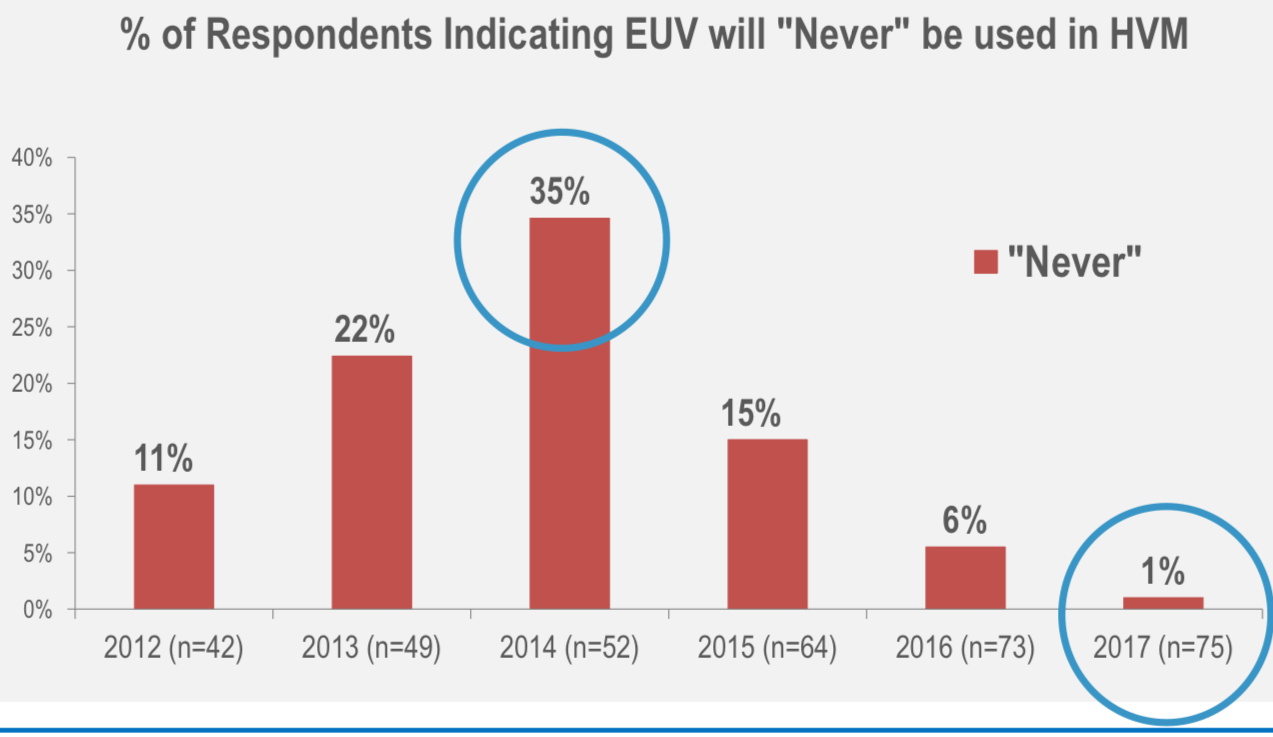
Fig. 1: EUV pessimism is now negligible. Source: eBeam Initiative survey
McIntyre: The 3400s are shipping. A handful of them are populating the field. They have demonstrated 250-watt power. That is quickly ramping up and is populating the industry. It does feel like from a tooling perspective that some of the barriers that we had a year or two ago have really been taken down. The infrastructure is largely getting in place. That could support the high-volume manufacturing start this year, but more likely sometime in the next year.
SE: Right now, EUV is targeted for 7nm in 2019. There are some challenges in terms of inserting the technology in the fab, right?
Levinson: Every new technology does not come up smoothly the first time in high-volume manufacturing. But putting it into manufacturing is often the best way to get those problems fixed quickly. It generates a sense of urgency. The technology has to be good enough so that we don’t completely fail. An analogy is what happened with immersion lithography. I remember that because AMD was the first one to put it into high-volume manufacturing. The big problem was defects. We basically had to get the defect levels down to a point where we could make commitments to customers. Clearly, it wasn’t at the point where we would be as profitable as we wanted. But by making that commitment, it just kind of pushed everybody to accelerate the activities to improve yield. The same thing could happen to EUV.
SE: One issue with EUV is the tool uptime. The uptimes with the EUV machines are hovering around 70% and 80%. What about this and other challenges with EUV?
Levinson: Where it is today is where people have decided that it’s acceptable to start. But we will use EUV lithography consistent with our ability to deliver to customers. So I may not use it on as many layers as I had originally wanted until the reliability is there. I haven’t bought more tools to compensate. But it definitely has a long way to go to be where we are with today’s optical scanners.
Freed: EUV is good for resolution. EUV will help by reducing some of the step counts. And in principle, that will help EPE (edge placement error). Anytime you reduce overlay steps, you reduce the amount of errors in the process. EUV comes with a stochastics penalty, however. So EUV will help in both resolution and edge placement error, but it won’t totally fix our edge placement error problem.
SE: In EUV, the term stochastics is a hot topic. In simple terms, EUV light or photons hit a resist, which causes a reaction. But each time, the reactions might be different. This results in random variations. The term stochastic describes something that consists of a random variable. Then, a variation from one event to another is called photon shot noise. But why is this all important?
McIntyre: It’s mainly related to the limited available photon density or how many pieces of information that are coming from the mask that you have to resolve an image in a particular place. You have local variability in the number of photons that are coming in, but you also have potential variability in the chemical elements that are sitting there waiting to interact with the photons. So these two things together lead to these variations. We’ve always had these variations. But the thing that has brought stochastics to the limelight is the fact that as you go to smaller and smaller features sizes, those variabilities, like the roughness right at the edge, has stayed somewhat flat for quite a while. So as the features gets small enough, what you find is that the CD distribution is no longer Gaussian. You start to have this asymmetric tail of the Gaussian distribution. That means you have some increased probability of these failure events. So as we get to smaller features, our stochastics rate or the number of failure rates are starting to increase exponentially. We’ve done a lot of work to try to dig into what are the main drivers of the stochastics. Dose is clearly the big one. Then, there are a whole bunch of other things that need to be optimized.
Hayashi: In EUVL, the mask 3D structure itself will affect the printing image. For example, you have sidewall angle types of issues. That may increase the stochastics error rates. Also, we don’t have a proper inspection method to accurately measure the parameters yet. So that’s one infrastructure issue. It’s a problem we still have.

Fig. 2: 3D Mask Effects. Source: BACUS Newsletter, GlobalFoundries, SUNY Poly, Lawrence Berkeley National Laboratory, Imec
Freed: When we look at wafers with stochastics, what you start seeing in etch is that you have resist profile variations. And the resists are very thin. So when we etch that, there are risks that you start etching through some of the areas in the resists. The other thing that we start seeing is scumming, footing and changes across the wafer. And so all of those things together cause opens and shorts. So we are looking at ways of fixing some of that by pro-processing in etch.
SE: In addition, there are several mask challenges in EUV. For example, the industry must use optical and/or e-beam inspection for EUV masks, but both technologies have some limitations. The industry wants actinic pattern mask inspection, but no such tool exists. Can we live without actinic pattern mask inspection? And what about EUV pellicles?
Hayashi: We need several years to obtain an actinic inspection system for EUV masks. In the meantime, we need to inspect EUV masks before shipping them to prevent killer defects. Currently, we can use deep UV-based defect inspection systems. And recently, ASML released a multi-column e-beam mask inspection system for EUV. Still, e-beam inspection systems have a throughput issue. They can inspect within six hours. It’s maybe 2X longer compared with current optical inspection systems. In that case, maybe we need to combine print check and current inspection capability technology.
Levinson: Clearly, we are some distance away from a HVM-quality pellicle. So we will have to find alternative methods of qualifying masks until they are ready. The impact is productivity. So the full benefit of EUV won’t get realized until we solve these last problems. So, the four companies that have made commitments to use EUV in manufacturing are all at the point of saying: ‘We just have to get started.’ That’s the way we get the remaining problems fixed more quickly. And one of things we are compromising is having the lack of a pellicle. Some years ago, the first products I used were g-line steppers. They did not have pellicles. That was not easy. But it got things started.

Fig 3: Pellicle prototype. Source: ASML
SE: What else can happen?
Levinson: We know that the reticle will get dirty inside an ASML tool after 20 to 25 reticle exchanges. So what you need to do is you expose a lot of wafers, and then you need to do qualification of the mask before you etch those wafers. One of the reasons why we like the concept of EUV is to improve cycle time over multiple patterning. But I’m losing my cycle time now for the mask qualification. So we quickly need to get that pellicle. In comparison, 193i is tens of thousands of exposures. It’s a different set of problems. Because you have a pellicle, you don’t worry about fall-on particles. But there have been contamination issues. There have also been degradation issues of the absorber.
Fujimura: So it’s two or three orders of magnitude difference. That’s a lot.
SE: Is the mask infrastructure getting ready for EUV?
Fujimura: There is clearly a lot more activity since maybe last year. There has always been a lot of interest. When you go to mask conferences, there have been a lot of papers on EUV. But in actual activity, there is no question that EUV masks are a first order project at all of these leading-edge companies now.
SE: There are several signs that the EUV mask industry is getting ready, especially for mask writing. For example, mask makers use single-beam e-beam tools to pattern or write the features on a photomask. But the write times continue to increase for the most complex masks. This is especially true for EUV masks. Now, the industry has developed multi-beam mask writers. What does multi-beam bring to the party?

Fig. 4: Multi-beam uses many beamlets in parallel. Source: IMS
Fujimura: Typically, multi-beam mask writing is thought to be great because it’s shot count-independent. It doesn’t matter about the complexity of the shapes. It can write a mask at a constant time. But the other thing that’s actually more important is that it’s very good for low-sensitivity or slow resists. So when you have EUV, you might have 100 microcoulombs per centimeter square, or even greater. Depending on how small a shape you want to be able to write, you have to use slower resists. The slower the resists are, the bigger the difference will be for the multi-beam systems. This is because multi-beam scatters the electrons more. Because of that, you don’t have a heating problem. So you can write with the same number of passes, whereas if you write it with a VSB machine, you have to write it with more passes than you are used to. Multi-beam is really good for complex shapes, but also for drawing smaller shapes that EUV requires.
Related Stories
Looming Issues And Tradeoffs For EUV
Searching For EUV Mask Defects
Next-Gen Mask Writer Race Begins
Challenges Mount For Photomasks
Unsolved Litho Issues At 7nm
Survey: Optimism Grows for EUV
 |
 |
 |
|
 |
 |
 |  |
The 3D mask issue is subtle and insidious. Different features on the mask focus very differently, apparently cannot be on the same mask.
Some paper in SPIE conference shows potential solution to this issue, e.g. by through process-window source mask optimization or OPC. Yet it is still very tricky and complicated considering the stochastic shot noisy effect and the stringent mask rules for dense and smaller patterns. Besides shadow effect, optical proximity effect, flare and multilayer defect, all need carefully handling.