Increased interactions and customization drive up risk of re-spins or failures.

Cramming more and different kinds of processors and memories onto a die or into a package is causing the number of unknowns and the complexity of those designs to skyrocket.
There are good reasons for combining all of these different devices into an SoC or advanced package. They increase functionality and can offer big improvements in performance and power that are no longer available just by shrinking features. But all of these elements also take up space, no matter how small the individual components. In fact, it’s not unusual for the most advanced planar chips to exceed the limits of a reticle, requiring different die to be “stitched” together to provide more real estate. These various functional elements also greatly increase the complexity of a device. Ironing out potential conflicts and other problems caused by rising complexity across a larger chip surface, or between multiple chips in a package, is becoming a massive challenge.
In the past, a chip included a processor, on-chip and off-chip memory, and I/O. Now it may include a collection of multi-core CPUs, GPUs, FPGAs, eFPGAs and other specialized accelerators, MCUs, DSPs, and NPUs. It also may include various flavors of DRAM, MRAM, SRAM, and flash memory. And it can include multiple I/O options, some for short-range communication, others for mid-range and longer-range communication, each with different frequencies and signal isolation requirements.
Making matters worse, these designs are being customized for specific markets and applications. Until a couple of years ago, when the vast majority of chips were designed for computers or smart phones, engineering teams were able to work the bugs out of every device and address most of the unknowns in those designs. That’s no longer true. Advanced chips are being designed in the context of much bigger systems, such as cars or specific cloud operations, and they are interacting in new ways that are not yet fully understood.
All of the big EDA vendors have quantified these issues differently, but the trend lines are similar. Each shows dramatic upswings in complexity regardless of how they slice the data — and many more potential problems as a result.
Ansys, for example, focuses the number of unknowns, which increased from about 700,000 in 2000 on a 0.1mm² die, to 9.5 million unknowns in 2020 for a 2mm² chip, and 102 million unknowns this year for a 30mm² (1.18 inch²) chip (see figure 1).
“What you would really like to do with ICs is design them in the context of a system,” said Rich Goldman, director at Ansys. “What we’ve been doing is designing the chip and then building the system around it. It’s about what can you do with this chip. But when you look at the systems companies, they’re designing the system first and then building the chip. So now you need to be able to simulate the chip in the context of the entire system.”

Fig. 1: Unknowns increasing over time and with increased size and complexity. Source: Ansys
Synopsys points to similar issues using a different data set. It highlights the complexity of designs with heterogeneous compute, as defined by the number of elements and corners, which has increased more than 100X over the past several years (see figure 2).
“When you come up with the origin of devices, you have a C-V (capacitance-voltage) curve, an I-V (current-voltage) curve, and you have device models that try to predict it,” said Aveek Sarkar, vice president of engineering at Synopsys. “It’s becoming more and more complex to model all those parameters. And now we have customers coming to us and asking, ‘Do you really need to operate off that model? Or can you go more upstream, because there is so much guard-banding that is built into every model? In the past we could have that headroom, but now we can’t. So can you go upstream with some of the data used to create the model, and start off with that?'”

Fig. 2: Complexity due to heterogeneous computing. Source: Synopsys
Siemens EDA points to a similar trend from perspective of re-spins, particularly due to analog circuitry (see figure 3). This is noteworthy because of the increasing amount of analog/mixed signal content in chips, notably with power electronics and sensors.
“What is going on is that the industry continues its migration to advanced nodes, where variability is extremely difficult to model,” said Harry Foster, chief scientist for verification at Siemens EDA. “On top of that, these models are evolving with the process. There are lots of corners to verify. But a more interesting trend is that we are seeing an increase in the number of complex mixed-signal designs, regardless of technology node, as companies try to optimize the area footprint to include analog.”

Fig. 3: Causes of respins over time, with a huge a spike due to analog. Source: Wilson Research Group/Siemens EDA
Scaling in three dimensions adds yet another level of complexity. Architectures have shifted up and out to be able to stuff more compute capability into a package, rather than onto a single die, but that has added its own set of complexities (see figure 4). While it’s possible to put everything into one die, or at least a stitched die, it’s faster to connect them together using an interposer or some type of bridge. Previously, this approach carried a performance and power penalty, but floor-planning in three dimensions using fatter pipes can shorten the distances that signals need to travel using less drive current.
“Moving to More-than-Moore means many more tools are required in the flow,” said John Park, product management group director for Cadence’s Custom IC & PCB Group. “In particular, top-level planning requires multiple system-level (multi-chiplet) analysis tools. These tools are new to SoC designers, and flows are more complex than ever.”
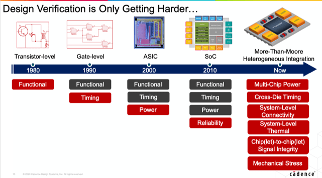
Fig. 4: Verification challenges in advanced packaging. Source: Cadence
Dealing with complexity
Within a leading-edge chip or advanced package, both of which are being customized for specific applications or markets, complexity needs to be dealt with almost on a one-off basis. What’s changed is that many of these designs are no longer being produced in billion-unit volumes. Even derivative chips may look very different from the original architectures.
For systems vendors developing these chips, the cost can be spread across total system development and, in some cases, amortized against operational costs. So for a large cloud operation, improved performance and lower power can reduce the number of required server racks, which in turn impacts the amount of real estate needed for a data center and the cost of powering and cooling those machines. For an automotive design, an advanced AI chip may be used across multiple product lines, and at least in theory, for multiple model years.
Nevertheless, there is constant pressure to simplify the development process and reduce the overall cost, which can be in the hundreds of millions of dollars for a single advanced chip. To this end, tools vendors have been working to identify horizontal or common problems that crop up across multiple vertical markets or implementations. Many of these efforts are built around standards that already exist, and new ones that are being developed.
“There are several aspects that need to be considered, such as making sure the customer is using the right version of the IP,” said K. Charles Janac, chairman and CEO of Arteris IP. “You’re basically enforcing that the IP-XACT parameters are there in order for the IP block to be admitted into the SoC. There’s also the aspect of supply management. Many of these companies have a layout house, a design house, and foundry contractors. If that entire supply chain is IP-XACT — from the interaction between the various parties in the supply chain to what ultimately provide what goes into the SoC — it gets much, much smoother. At the same time, you are going to have some pieces of the chip that are on the leading-edge process and some on the trailing edge, such as analog. For mixed signal, it doesn’t necessarily sense to have it on 5nm or 3nm, but it does for the processing system. And so you wind up with chiplets, system-in-package, and with IP-XACT for the configuration of the exit ports, which eases that process. So with inter-chip links that are compatible with the NoC, we can make the chiplets look like a single programming space to the software programmers.”
The challenge is being able to fuse all of these pieces together into a high-level abstraction, and then drill down to make changes that can be analyzed at the higher level. This is where much of the big EDA companies have focused their efforts over the past several years. EDA vendors have been increasing the speed and capacity of their tools and equipment, including utilizing heterogeneous platforms for accelerating various steps in the flow, sometimes combined with machine learning.
In addition, all of the major tools vendors have been leveraging the cloud whenever extreme amounts of compute power are required, such as during verification or debug. The result is that simulation, emulation, and prototyping now have far more headroom than in the past, and there is much tighter integration between point tools and those higher-level platforms.
Thinking much bigger
One new challenge in the increasingly complex design process involves different data formats. Multi-chip implementations and system integration generate more data throughout the design-through-manufacturing flow, but not all of that data understandable by different tools. Being able to integrate all of that data would allow for a much simpler flow.
“You need to standardize data formats so that you’re able to exchange information between simulators, allowing you to use a generic interface for analyzing data formats,” said Roland Jancke, department head for design methodology at Fraunhofer IIS’ Engineering of Adaptive Systems Division. “If all the pieces refer to standardized interfaces, then the chance they will work together is higher. This is true for the development itself and for the development process. So we have to develop certain products, but before designing the product we have to build up models out of the parts. If those models fit together, and if we have a chance to see whether the models of those parts work together, then we can be sure the system itself will work later on.”
Raising the abstraction level using consistent data formats is a challenge, though. It requires cooperation across the supply chain. More disciplines need to come together earlier in the design cycle to make sure that a device can be inspected, tested, and that it will yield sufficiently. Designing a complex chip now requires expertise in electrical engineering, verification, test, power, mechanical engineering, software, as well as domain experts, and in some cases data scientists with expertise in machine learning, deep learning, and AI.
“In the past, these teams didn’t talk,” said Hany Elhak, group director for product management and marketing at Synopsys. “They used different tools and they used different flows. Now they have to talk. So from the EDA side, we need to be cognizant of that. We need to provide converged workflows that allow these teams to work with each other. We are trying to address two problems. There is the traditional one, which is those circuits are now bigger and more complex, running at higher frequencies, and they have more parasitics. This is the scale problem, and we are trying to deal with this by offering faster simulation and higher capacity simulation. The other problem, which we are trying to solve, is that now you have many different types of circuits that are part of that bigger system, and they need to be designed together. For that we need to have some common flow for these different design teams so that we don’t end up with problems at the end of the design cycle when we try to connect these things together.”
A second challenge involves the inclusion of AI/machine learning in an increasing number of devices. AI depends on good data and consistent formats to achieve accuracy levels that are sufficient for whatever task it is used for.
“The accuracy piece is challenging in and of itself,” said Rob Aitken, Arm fellow and director of technology. “The score you get on some standardized puzzle or data set isn’t necessarily indicative of what it’s going to do in its real application. So if it identifies 95% of images correctly, but your application is all of the 5%, then you’re stuck.”
Predicting accuracy is even more complicated in a multi-function system.
“If you have a system with a given accuracy, and a different system with another, their overall accuracy depends on how independent the two approaches are from one another,” Aitken said. “But it also depends on what mechanism you use to combine the two. This seems to be reasonably well understood in things like image recognition. But it’s harder when you’re looking at, say, an automotive-type application where you’ve got some radar data and some camera data. They’re effectively independent of one another, but their accuracies are dependent on external factors that you would have to know, in addition to everything else, in order to actually say, ‘The radar says it’s a cat, the camera says there’s nothing there at all.’ The reality is that because it’s dark, the radar is probably right. But if it’s raining, maybe the radar is wrong, too. These external bits come into play very quickly and start to overwhelm any rule of thumb you might have.”
Building systems
To add confusion on top of confusion, a chip or a package now needs to work in the context of a bigger system even though the chipmaker may not have any insight into that larger system. This is like designing for a socket without knowledge of the end product, but on steroids. Designing a unique chip or package now requires the context of a unique system, and systems of systems, and it is forcing tools and IP vendors to look at problems differently. Essentially, they need to either take a top-down approach to encompassing all of the underlying issues, or they need to find a horizontal solution that applies across multiple vertical market implementations.
Consider, for example, the design of AI chips and systems, which are almost all unique.
“When we build a PHY, for example, we want to sell it as many times as we can,” said Steven Woo, fellow and distinguished inventor at Rambus. “So we build it across this big range of use cases. That’s partly because it’s really expensive to build, design and develop a PHY. You’ve got to try and sell it a lot. In the case of AI, what we’re now is people are really targeting pretty specific use cases. It doesn’t mean they can’t be used across a range of applications, but some of the software nature of it allows you to do much more fine tuning on a particular type of application than in the semiconductor industry. We’re trying to make things very general. It’s a different kind of approach.”
Focusing on system design adds a whole new set of challenges, though. Instead of variation in a chip, for example, there is the potential for additive systemic variation. Put simply, variation in a multi-chip package may be the sum of variations of different chips, some of which may be developed using entirely different processes at different dimensions and even from different foundries.
“What we see from standard chip variation is well understood, and there are methods available to deal with these variations,” said Andy Heinig, group leader for advanced systems integration and department head for efficient electronics at Fraunhofer IIS EAS. “But on the package side, we assume there will be new problems. They are not known up until now, and systems will fail because you only see these new problems if you measure something. At that point you can do something to deal these problems. But it may be a combination of different problems that we haven’t had up until now, and while some of the problems are known and understood individually, they’re not in the combination of a system.”
More choices
All of this extends well beyond just a single vendor. The supply chain is complex and global, and not all technologies mature at the same rate. In a heterogeneous design involving multiple vendors, the choices can vary greatly from one design to the next.
“With 5nm or 7nm technologies, you see logic processes moving to those very advanced processes, but the memory technologies may not move as fast as the logic technologies do,” said Douglas Mitchell, vice president of the RAM Business Unit at Infineon. “So it may be very appropriate to have a memory technology that has decades of experience behind it, but which won’t be down at 7nm anytime soon. It can use separate chips to optimize tradeoffs between reliability and performance and costs.”
This is particularly evident at the rapidly evolving edge, where solutions are being customized for specific applications and domains.
“Especially in edge compute environments, we’re going to see different combinations of requirements,” Mitchell said. “You’ve got a processor, data logging memories, code storage, and real-time processing expansion memories. All of these have different characteristics, and you’re trying to optimize different metrics. You may want to have some kind of a data logging memory that has very high-endurance cycle life because you want to be able to capture data at real-time clock rates for 20 years in the field. So it’s got to have certain characteristics. Flash memory may have to store code under harsh environments and implement security features. So there are different combinations of things that are going to be combined in these edge network devices. And if you can embed some of the machine learning capability out at the edge node, then you can do a lot of the real-time processing and decision making at the edge and make those decisions on what data needs to be sent to the cloud. So it is a complex problem with multi components to consider.”
The complexity also adds issues of keeping track of all of the IP used in these designs. “We’re definitely seeing a lot more traction from the semiconductor IP providers,” said Simon Rance, head of marketing at ClioSoft. “They’ve had this concern for 10 years, but it’s growing and escalating. This started with multiple uses of IP, especially with legal agreements. Especially for the bigger IP companies, the high-end IP costs a lot. A lot of companies buy a per-use license. The problem is that it can’t be policed by the IP provider. It’s legally bound, but they don’t know if it’s getting used on more than one design. The bigger companies don’t want to buy an IP from an IP provider and break those legal agreements, and that can happen very easily. And a designer has no idea in a company has no idea if it’s a one-time license. We’re seeing a lot of IPs held on file servers. They’re not locked down. There’s a management issue that’s missing, which is what we’ve been addressing.”
Conclusion
The complexity of chips has been increasing for some time, but for the most part it was held in check by the economics of Moore’s Law. As those economics change at the most advanced nodes, chip architects are creating a number of options to greatly improve performance and optimize performance per watt. While this has given rise to a period of creativity and spawned many new options, the amount of customization and the growing size and complexity of chips also has made it harder to check everything with today’s tools and to leverage previous learnings.
“We’ve been running with Moore’s Law for more than 50 years, and that’s all about semiconductors,” said Ansys’ Goldman. “But in order to design those semiconductors, you need the EDA that supports it. We’ve had great innovation as a result. But now we’re seeing exponential innovation, and the number of unknowns is increasing with it.”
Getting a handle on these exponential shifts will be the big challenge of this decade, and it will define how advanced chips are designed, manufactured, and tested — as well as how well they perform throughout their projected lifetimes.
Related
What Goes Wrong In Advanced Packages
More heterogeneous designs and packaging options add challenges across the supply chain, from design to manufacturing and into the field.
Hidden Costs In Faster, Low-Power AI Systems
Tradeoffs in AI/ML designs can affect everything from aging to reliability, but not always in predictable ways.
Performance And Power Tradeoffs At 7/5nm
Experts at the Table: Security, reliability, and margin are all in play at leading-edge nodes and in advanced packages.

 |
|
 |
 |
 |
 |
 |
 |
 |
 |
Leave a Reply