Multiple sources of variability are causing unexpected problems in everything from AI chips to automotive reliability and time to market.

Variation is becoming a bigger challenge at each new node, but not just for obvious reasons and not always from the usual sources. Nevertheless, dealing with these issues takes additional time and resources, and it can affect the performance and reliability of those chips throughout their lifetimes.
At a high level, variation historically was viewed as a mismatch between what design teams intend to be in a chip versus what actually shows up in the manufactured chip. Foundries provide a set of process rules, which are used by EDA companies and designers to adjust for those discrepancies. Design teams and fabs then typically add their own guard-banding to ensure the chip functions as expected and that all possible corners are addressed.
This approach is becoming more difficult to sustain on multiple fronts. The number of process-related corners has been rising steadily over the past four process nodes (see Fig. 1 below). Along with that, the tolerances for noise of all sorts have been going down at each new node due to increased power and transistor density, thinner dielectrics, and more circuitry that is always on.

Fig. 1: Process-related corners are increasing. Source: eSilicon
To make matters worse, there are more sources of variation, and there are many more types.
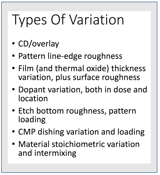
Fig. 2: Variation examples. Source: KLA-Tencor
“Variation comes in many different flavors,” said David Fried, CTO at Coventor. “Printing is a significant factor, and a popular topic. It’s not so much ‘broken lines,’ but lines that are nominally designed at the same dimension being printed and fabricated with slightly different dimensions, and therefore behaving differently (even though designers expect them to behave the same). And it’s not just lithography in this segment of the problem. Lithography, deposition, etch and clean all work together in the patterning aspect. But variation also comes in seemingly invisible ways. Sometimes you have some thermal variation across the chip or across the wafer that causes material changes, such as dopant diffusion, to be varied. This causes electrical behavior variation across the design, again unexpected by designers. There are a huge number of different ways that variation can be introduced. Understanding those mechanisms and parsing out their effects—cross-chip, cross-wafer, wafer-to-wafer—is critical to developing yielding technologies.”
Litho issues
Lithography is an obvious starting point for any discussion about process variation because it was the first place where variation became a major issue for the entire chip industry. The greater the transistor density, the more mask layers that are required, which almost guarantees that variation will creep into the process. That is true whether it involves EUV scanners, which can vary from one to the next, or the 193 immersion process, where multiple masks have to be overlayed to achieve a single image that could be done in one pass using EUV.
In addition to process variation, there are variations in the masks themselves. Photomasks are developed for a specification, and that spec includes an “error budget” assigned to the mask manufacturing process. So the mask incorporates the error budget for both the mask and the wafer processes.
“Standard cells and interconnect and vias and contacts are all designed according to design rules, which are in turn determined by carefully studying what can be manufactured reliably according to the wafer and mask specs,” said Aki Fujimura, CEO of D2S. “If process variation on the wafer can be contained to 0.1nm instead of 2nm, speed and power specifications of a standard cell (or any circuit) would have less variation in the specified corners. The corners, in turn, drive RTL design, synthesis, place and route to design a chip that will perform at the target speed, making sure that the signal goes from one clocked device (stage) to the next on time, and also that the signal stays there long enough for the next clock cycle to arrive. It’s an incredible coordination of many different people in a chain of exchanges of specifications of allowed tolerances and error budgets that allow semiconductors to be designed and manufactured reliably.”
One area of particular concern is how the various mask layers go together.
“The most critical factor limiting scaling isn’t resolution anymore, it’s edge placement error (EPE) caused by the movement of an edge in any direction which results in vertical misalignment between layers,” said Uday Mitra, vice president of strategy for etch products at Applied Materials. “Primary contributors to this are lithography sources of variation, including overlay, CD uniformity and line-edge roughness and process variations in etch and deposition. Process variability includes CD uniformity and profile shape uniformity. An example of variability challenges in a chip is the alignment of vias which can number up to 100 billion. A single misaligned via can impact reliability.”
In the past, the ITRS was used to coordinate error budgets and tolerances. Since it was abandoned, the industry has been struggling for a consistent way of addressing these problems. Statistical models are being studied for future development, but so far the industry is sticking with what it already has.
“For semiconductor processes to be useful, it has to be reliably manufacturable,” Fujimura said. “When people talk about 3nm node, they mean that 3nm devices can be manufactured reliably. There’s inspection and repair for masks, so that also increases reliability. There are devices with redundancy and error tolerances, so less-than-stellar manufacturing reliability is tolerated because of the design. This is a part of what makes a difference between what’s good for one type of an application but not for another. Nanoimprint lithography (NIL), for example, is only for Flash and other defect-tolerant applications.”
Materials
Lithography is just one slice of the variation pie, which is comprised of acceptable levels of distributions from a number of different areas. Increasingly, that includes materials, which has its own separate supply chain. At each new node, that becomes more difficult to deal with, as well.
“It’s like improving toward a moving target, because the bar has moved substantially before the previous level is fully understood,” said Julie Ply, quality engineering manager at Brewer Science. “The challenge is finding the source of the variation. Measurements are tougher and tougher at each node. So even before you figure out what’s happening at the previous node, now you’re onto the next node where the tolerances are 100 times tighter. On top of that, we may find more sensitivity in ions. That doesn’t mean variation was not there in the past, but we didn’t see it. Now everything is getting more stringent, but we’re also getting closer to the limits of metrology.”
And that creates a problem. “There are techniques for managing variability,” said Klaus Schuegraf, vice president of new products and solutions at PDF Solutions. “But to solve this you need to be able to see it. We’re big believers that if you can’t measure it, you can’t manage it.”
The entire industry has been shifting from pure observation through inspection and metrology to a combination of observation and data analysis. That is being augmented by machine learning, where the goal is to establish a distribution of acceptable variation parameters.
The biggest opportunity out of all of this is to be able to do predictive analysis,” said Brewer’s Ply. “This is an ongoing project for us. We want to be able to predict what the next batch of materials will do. Raw material data is one of the greatest sources of information. The more forthcoming a supplier is with data, the more aligned data is.”
Yield issues
Yield is perhaps the least understood aspect of variation because it’s not always a clear-cut cause and effect.
“If the variation is big, yield will be low,” said John Chen, marketing director at UMC. “Foundries always offer a PDK, which includes process variation, which basically is margin for a device. If process variation is big, the coverage needs to be huge and you need to enlarge the device.”
He’s not alone in seeing this. “In many ways, reliability is just the tail of the yield curve,” said Coventor’s Fried. “If you think of an interconnect line that is, for one reason or another, exhibiting higher resistance than expected (nominal), if that variation is small enough then the chip design can contain the effects. If that variation is large enough, the design will fail at test. But, somewhere between those cases is a range where the design will perform acceptably initially, but fail later on due aging or other time-dependent effects. This is termed a ‘reliability fail’ because it wasn’t caught at time-zero, but in many cases it stems from the same effects of yield degradation. As new designs come to fruition, failures will manifest in different ways, so having designs that are more diagnosable and more fault-tolerant will be really important. But as with most challenges, this will need to be solved with a combination of design, process and integration solutions.”
There are important business reasons for making that happen. Dealing with variation slows down the entire manufacturing process, which in turn increases the time it takes to burn through inventory. Moreover, yield isn’t as simple as a chip works or fails. Chips that don’t meet an OEM’s spec still may be useful in Tier 2 and Tier 3 products.
“If you observe the number of chips in bins 2 and 3 are too high, you can either increase inventory or increase risk,” said UMC’s Chen. “The risk is getting higher and higher. So variation can impact your entire business strategy.”
Variation also impacts different types of chips in different ways. The problem is particularly noticeable in some AI chips.
“From a performance standpoint, you’re worried about cross-field variation in your device performance in a critical path,” PDF’s Schuegraf said. “So you can wire out your transistors with a critical path to one side and another, and those need to be controlled with a certain tolerance. Cross-field is a major problem because some of these AI chips are full-field. The field size is about 600 or 700 square millimeters. That’s a huge die. So you’ve got device variability. And at 7nm the interconnect is very congested, so people have introduced an intermediate metal layer to relieve the congestion between the gate and the drain contact. The drain contacts are now bars (rectangle/ovals vs. square/circles), so you can achieve better contact resistance and less variability. The result is you have more capacitance between gate and drain. But when you have a metal bar in there, you have to add a contact onto the source and drain. The way you do that is to add another metal layer. That adds variability. The overlay is quite tight. So as that moves around, the resistance changes. As that overlay changes, the resistance changes. Now you have a whole new source of variability. So you’ve solved one problem and created another.”
And that’s just for AI chips, which tend to be arrays of the same logic and memory elements. Other chips have their own unique problems.
“For logic, the impact of variation is more about yield and leakage,” said Doug Anberg, vice president of advanced lithography applications in Veeco’s Ultratech Division. “For memory, it’s how you control and manage stress. And for 3D (packaging), there is a new focus on critical layers.”
Application-specific issues
While variation affects all process nodes, the biggest challenges are at the most advanced nodes because the processes are still not mature. This is particularly problematic in automotive electronics, where OEMs and Tier-1 suppliers are developing systems for assisted- and autonomous driving based on 10/7nm technology.
“One of the larger obstacles to zero defect success is the so-called ‘latent defect,'” said Rob Cappel, senior director of marketing at KLA-Tencor. “These defects may be of a size or location that does not initially kill the die, or they may lie in an untested area of the die, which is an increasing problem with complex SoCs. As a result, the at-risk die passes electrical test and ‘escapes’ into the supply chain. The demanding automotive environment of high heat, humidity and vibration can sometimes ‘activate’ these latent defects, causing a premature failure. The industry has long relied on electrical testing as the method to cull bad die, but latent defects pass electrical testing, so other methods are required to stop escapes near the source where costs are lower. Industry estimates have the cost of an escape increasing 10X for every layer of integration it passes (fab, test, board, system, car 0km, warranty, recall), creating a strong push to find the underlying latent defects in the fab.”
Cappel noted that variability is a large source of latent reliability defects—especially variability that is related to lithography patterning, which includes CD, overlay, line-edge roughness, and localized lithography variability. “These sources of variation can and do cause partial voids or bridges, which then can breakdown in the extreme automotive operating environment. The same can be said of any patterning issues with etch (partial etch) and CMP (CMP dishing). Basically increased variability in a process leads to smaller process windows and more yield and reliability failures. Variability has to be significantly reduced in a zero-defect program, and it becomes significantly harder as the design rules shrink.”
There seems to be widespread agreement on that point. “It gets worse for sure at the most advanced nodes—a lot worse,” said D2S’ Fujimura. “That’s why more and more types of simulation and verification are required over time. The stochastic noise problem of EUV at some node in the future will be yet another significant factor. But when the fab is ready for 5nm, that means they are ready to manufacture designs that adhere to its design rules reliably. So, in that sense, the problem doesn’t get worse. But that’s by definition. I guess you could say that the challenges get a lot worse, but they’ll amazingly make it so the chips are still reliable in the end, despite the increased variation.”
Still, automotive adds some unique twists because of the environmental extremes and the safety-critical design requirements.
“Variability can impact reliability like TDDB (time-dependent dielectric breakdown),” said Applied Materials’ Mitra. “Reliability requirements are higher for some chips, like the ones used in cars, so avoiding mis-alignment of features is critical. There are physical limits to how well we can control processes, so all devices will have a certain amount of variation. The only solution is to make the key parts of the device, like the vias and contacts, insensitive to this variation. Self-alignment is critical to resolving EPE, and we see the industry rapidly moving to self-aligned techniques to form various structures, such as gate contacts and vias. But this requires new materials. Litho-based solutions are just not sufficient. And with advanced nodes posing challenges for all device types, materials-enabled solutions with selective capabilities are now essential to continued scaling.”
This marks a big change for the automotive industry, in particular, where advanced-node chips are being used in the logic of assisted and autonomous designs.
“Automotive used to be a lagging technology,” said PDF’s Schuegraf. “With self-driving cars and ADAS, you need AI. You need high-performance computing under the hood. Reliability, multi-chip and automotive are the big problem areas. So the question is how you find reliability faults. We’re doing work there on PPM/PPB levels to find defects in manufacturing. Classic reliability is a bathtub curve. What if you never get to that low failure rate at burn-in? Do you take the risk and ship the product? How do you optimize the burn-in period?”
Not everything in automotive is moving to smaller nodes, however. In some cases, technology is moving in the other direction because of variation. Still, this requires some complex tradeoffs.
“You can minimize every variation effect with six-sigma design,” said UMC’s Chen. “But you also can achieve the same with three-sigma at an older node. The chip is bigger, but it’s more stable and you can minimize variation. So on a 12-inch wafer, you may get better uniformity in the center, but around the edges this is more difficult. If you move from 300mm to 200mm you minimize the variation.
Other issues
Finding variation-related issues when something can be done about them is harder than figuring them out after the fact, when data that is collected during manufacturing can be analyzed.
“No inspection or test system is perfect,” said KLA-Tencor’s Cappel. “But the latent defects that cause automotive IC reliability failures are directly related to random defectivity. Fabs have a significantly higher probability of catching these reliability issues inline if the appropriate inspection tools, sampling strategies and methodologies are used to find and reduce random defectivity. The best first approach to manufacturing devices with fewer overall defects is to closely control the process by employing continuous improvements programs that reduce the random defectivity introduced by the process tools or environment. This requires implementation of fundamental baseline yield improvement techniques – tool monitoring and partitioning. While fabs have used these strategies for years, they now must be raised to a higher standard in order to achieve the lower defect levels necessary to improve IC reliability. The second approach is to ensure that the process is sampled frequently enough to provide traceability. When the inevitable process excursion happens, zero-defect fabs know definitively where the problem started and stopped, and can quarantine the affected parts until they can be effectively dispositioned or culled.”
There are other effects, as well, that aren’t in the rule decks.
“Higher variability means you need more power to overcome,” Schuegraf said. “Essentially if VT or resistance are variable, you need to design for the worst case situation (high VT or high resistance). This requires higher VDD or bigger devices (more IDSAT). So in both cases, you increase the power requirement.”
That can cause its own issues, though. “There are some issues that are ‘over-time’ effects like electromigration,” Fujimura said. “These problems happen over time, so they pass initial testing, but fail in the field over time. In many ways, these are worst kind of error. There are EDA tools that catch these errors, so the design can be corrected before it is manufactured. However, most manufacturing variation issues are not ‘over-time’ effects. The statistical variation causes a geometric instance to fail (or to be sufficiently different from the desired shape), so it performs abnormally from the get go.”
Conclusion
Variation is not a new phenomenon, but it certainly is an increasingly important issue.
“Many of these challenges are effectively invisible,” Fried said. “Also, with the complexity of designs and technology now, you often are unable to sample enough area in your inspections to really catch all the defects. As technologies get smaller and more complex, this challenge gets bigger.”
While this won’t curtail designs at the most advanced nodes, variation imposes yet another set of hurdles that drive up the cost. And while some of this could be ignored in the past, a lot more people are paying attention these days.

 |
 |
 |
|
 |
 |
 |  |
7/5 nm is now believed to require multiple patterning even for EUV.