This technology has resurfaced as one option at 5nm, but it’s still not clear if it will work.

For years, the industry has been working on an advanced technology called area-selective deposition for chip production at 5nm and beyond.
Area-selective deposition, an advanced self-aligned patterning technique, is still in R&D amid a slew of challenges with the technology. But the more advanced forms of technology are beginning to make some progress, possibly inching closer from the lab to the fab.
The concept behind the technology isn’t new. For decades, chipmakers have used deposition, a process that deposits a blanket of materials on a surface. In area-select deposition, though, the idea is to use atomic layer deposition (ALD) to deposit materials in exact places. Using a bottoms-up approach, area-selective deposition, sometimes called area-selective ALD, is used to pattern and self-align tiny features on devices. Potentially, it could reduce the number of lithography and etch steps in the manufacturing flow.
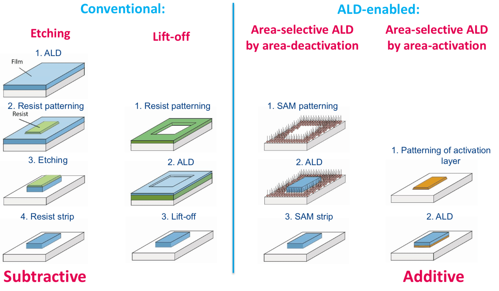
Fig. 1: Conventional patterning vs selective ALD Source: Adrie Mackus, Eindhoven University of Technology
For years the industry has used various forms of selective deposition in the fab to deposit metal materials on metal surfaces in devices. But for the more advanced forms of area-selective deposition, a tool must deposit different combinations of material sets in chips, such as metals on dielectrics, dielectrics on metals and dielectrics on dielectrics.
That’s the big stumbling block in R&D and the fab. For these apps, the tools or processes don’t exist, at least in production. However, there are challenges to make these material sets work with high selectivity and good yields. Generally, the mechanisms behind the technology are complex and not well understood, and for some time progress has been slow. It doesn’t help that demand for the technology has cooled as chipmakers are finding ways to extend existing techniques. There are skeptics who believe the technology is too far out or will never work.
The mood is beginning to change in the field of area-selective deposition, however. “Everybody has it on their radar screens,” said Efrain Altamirano-Sanchez, a principal member of the technical staff at Imec. “It’s definitely moving forward. The progress is slow, but steady. We are starting to understand certain parts of the mechanisms for area-selective deposition. For me, that’s one of the key elements. Once we understand the mechanisms, then things are going to align quite fast.”
Clearly, the industry is working on the technology for 5nm and beyond. TSMC, for example, recently announced a breakthrough in the arena. In addition, Applied Materials, Lam Research, TEL and others are developing selective deposition tools in R&D. It’s still unclear when the technology will appear, as the industry is keeping their efforts close to the vest.
Patterning challenges
For years, the industry was able to scale the traditional planar transistor with relative ease. Then, at 22nm/20nm, chipmakers encountered problems on several fronts.
Lithography, the key manufacturing technology that prints the features on devices, reached a tipping point. Extreme ultraviolet (EUV) lithography, a next-generation patterning technology, wasn’t ready. In addition, the latest lithography scanner, based on 193nm wavelength technology, reached its physical limit at an 80nm pitch, or 40nm half-pitch.
The industry solved these issues. At 22nm/20nm, the industry combined today’s 193nm lithography with multiple patterning. In multiple patterning, the idea is to use a sequence of process steps to scale the feature sizes of a chip. The best-known examples are self-aligned double patterning and self-aligned quadruple patterning.
Multiple patterning extends IC scaling, but it also increases the number of steps in the process. At each node, a chipmaker must also process more layers using a series of masking steps in the flow.
A 28nm device has 40 to 50 mask layers. In comparison, a 14nm/10nm device has 60 layers, and that number is expected to rise to 80 to 85 at 7nm.
Then, the device features become smaller at each node. On top of that, the features must be precise and placed on the exact locations on each layer of a device.
So, it becomes more difficult to align the various features and layers. Simply put, a feature or features may end up in the wrong place in a pattern, resulting in what’s called an edge placement error (EPE). EPE is measured as the difference between the intended and printed features in a layout. EPE can impact the yield of a chip.
In fact, back in 2015, Yan Borodovsky, the former director of advanced lithography at Intel, warned that EPE would become the limiter to Moore’s Law. (Borodovsky is now retired from Intel.)
At the time, Borodovsky said that the existing lithographic solutions would not solve all of the EPE issues in designs. To address the problem, he urged the industry to develop a novel technology called area-selective deposition.
So the industry began to work on selective deposition, but the technology proved to be a big challenge. “Selective deposition is very challenging. It’s like trying to control where each snowflake should land during a blizzard. How do you make sure the snow only covers the rooftop and not the street? The ability to use materials engineering to define the different features is critical,” said Ellie Yieh, vice president and general manager of Advanced Product Technology Development at Applied Materials, in a recent interview.
Meanwhile, the industry continues to use the existing patterning techniques, such as SADP/SAQP. But the traditional approaches face some EPE challenges at 10nm/7nm.
As a result, the field of selective deposition is heating up amid the push toward 10/7nm and beyond. “We’ve started to pay more and more attention to selective deposition. The reasons are quite clear. For a lot of scaling issues, selective deposition can enable future scaling. This is not only for the backend-of-the-line, but also for the front-end-of-line,” said Larry Zhao, a technical director at Lam Research, at the recent IEEE International Interconnect Technology Conference (IITC).
Selective deposition won’t replace existing or future patterning solutions. If it works, it would give chipmakers another technology in the patterning toolbox.
As previously promised, it could help solve some of the EPE issues in future designs. For example, current and future transistor types are becoming more three-dimensional in nature. In chips, the contacts and vias are moving in the same direction.
“Most of the trends in the architectures are pointing towards 3D. That’s true for both logic and memory,’’ said Kandabara Tapily, a researcher at TEL, in a presentation at IITC. “We are looking to go more and more toward the vertical direction, and to go to silicon nanowires/nanosheets or CFETs. In order to achieve that, advanced patterning will be a key to continued scaling.”
Nanosheets, nanowires and complementary FETs (CFETs) are next-generation transistor types. To pattern these types of devices, chipmakers will require various lithographic techniques.
But in many parts of the devices, chipmakers will lean more heavily on deposition and etch. But for advanced nodes, they will require new technologies. “We believe selective deposition and selective etch will be fundamental for those nodes coming,” Tapily added.
Selective etch involves atomic layer etch (ALE). Offered by several vendors, ALE selectively removes targeted materials without damaging other parts of the structure.
ALE works with other tools for both logic and memory. In the future, ALE will also work with area-selective deposition, if the newfangled technology ever appears.
What is selection deposition?
Selective deposition isn’t new. For years, chipmakers have used epitaxial reactors to deposit films on surfaces. Epi is a form of select deposition.
There are other forms as well. For example, on top of the transistor, chipmakers create tiny wiring schemes or interconnects in devices. Using electroless deposition or other techniques, a capping layer is selectively deposited on the structure to prevent electromigration.
At IITC, Lam Research presented a paper that expands the use of electroless deposition, a form of selective deposition. Lam described a prefill process for use in depositing cobalt in vias.
For this and other apps, the industry has mastered the ability to selectively deposit metal materials on metal surfaces in chips.
The industry also wants to deposit metals on dielectrics and dielectrics on metals in devices. That’s where area-selective deposition comes in. Combining ALD with specialized chemistries or precursors, area-selective deposition promises to deposit these and other material sets in devices.
That’s the big challenge. Generally for these apps, area-selective deposition or any other existing fab tools have yet to work consistently in both the lab or fab.
“Some options, such as metal-on-dielectric in the presence of metal, or dielectric-on-metal in the presence of dielectric, are extremely challenging,” according to Erwin Kessels and Adrie Mackus, who are professors at the Eindhoven University of Technology. “This is because once the deposition starts, you obtain two areas with a similar chemical character (i.e. metals on both surfaces, or dielectrics on both surfaces).
“Another big issue is defectivity,” according to Kessels and Mackus. “Some processes seem to work quite nicely in the research lab. But the selectivity is just not good enough to deposit sufficiently thick films, to have selectivity over large areas, and to have reliable processes in general without significantly compromising the yield. Defects play a very important role here as selectivity is generally lost at such defect sites.”
Still, the industry continues to move forward with the technology, which resembles today’s ALD. Used in today’s fabs, ALD tools deposit materials layer by layer at the atomic scale. ALD involves a binary process with two reactants—A and B. The first reactant, A, is pumped into the ALD chamber. The wafer is processed and then the chemistries are purged. Then the second reactant, B, undergoes the same step.
Typically, though, ALD deposits films on the entire surface, not in select places. So, for area-selective deposition, the industry requires a modified ALD tool or a new system built from the ground up. Area-selective deposition also uses ALD, but it’s different than traditional ALD. The difference is you trick the ALD process, so that it grows on material A, but does not grow on material B.
The main challenge is to understand and control thin-film nucleation. “We all know that nuclei form on surfaces and they have different shapes. They have different sizes and they grow,” said Gregory Parsons, a professor in the College of Engineering at North Carolina State University. “The surface energies drive the formation of these nuclei. The fundamental physics of this is understood in terms of this energy balance.”
The key is the initial reaction between the molecule and the surface. “That’s what we are talking about here is, how does that molecule interact with that surface during the first ALD step. That’s the real challenge,” Parsons said.
Meanwhile, there are three main approaches or ways of implementing area-selective deposition—selective precursor adsorption; selective co-reactant adsorption; and selective functionalization, according to the Eindhoven University of Technology.
Selective precursor adsorption is where an ALD tool will selectively grow a material on one area of a surface, but not another.
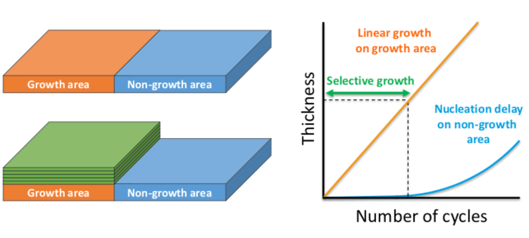
Fig. 2: Area-selective ALD on a specific material. Source: Adrie Mackus, Eindhoven University of Technology
Selective precursor adsorption is more complex. In this case, for example, you might use a molecular gas as a co-reactant. A material may grow on the surface where the co-reactant exits, but not on other parts.
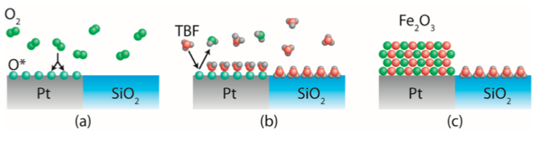
Fig. 3: Area-Selective Atomic Layer Deposition of Metal Oxides on Noble Metals through Catalytic Oxygen Activation Source: Chem. Mater. 2018, 30, 663−670, Stanford, Eindhoven University of Technology, Chonbuk National University, Toyota
Selective functionalization is where a tool will grow self-assembled monolayers (SAMs) on a surface. A SAM forms a tiny mask. Then, the desired material is deposited on the surface. The material nucleates on the surface not covered by the mask.
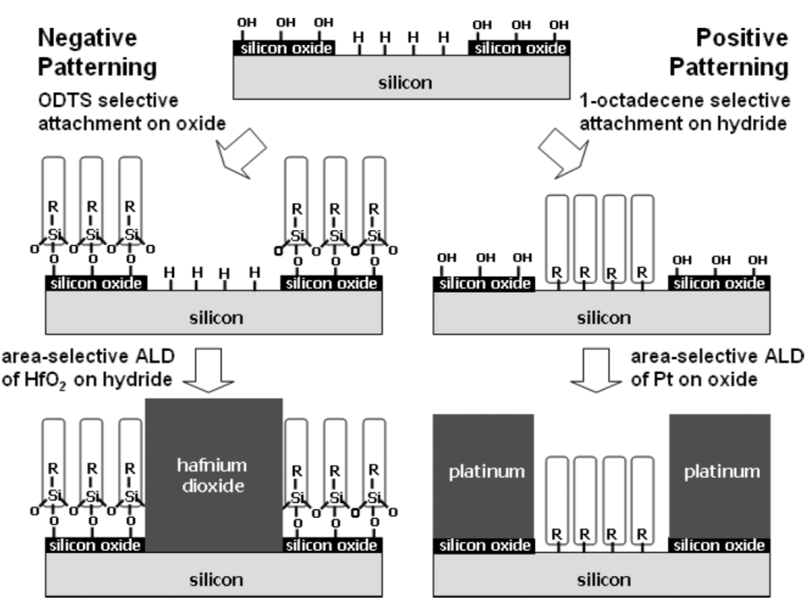
Fig. 4: Selective deposition using SAMs Source: Adrie Mackus, Book chapter: Nanopatterning by area-selective ALD, Lee and Bent, in ALD of nanostructured materials, Wiley, 2012
With these and other approaches, there are still several challenges. For example, in one application, you want to deposit a material in one area and not another.
During the process, however, the selectivity is sometimes lost. The area that is targeted for non-growth sometimes undergoes unwanted changes, according to researchers from Eindhoven University of Technology.
One solution is to add correction steps in the flow. “Since conventional ALD processes typically do not provide the desired selectivity, partly because the non-growth area changes during the deposition, current efforts in many research groups focus on the implementation of correction steps, such as dosing inhibitors, or etching unwanted material from the non-growth area,” according to Kessels and Mackus from the Eindhoven University of Technology.
One correction step involves the use of ALE, which would work with selective deposition. ALE removes unwanted materials in the non-growth or other areas.
Dosing inhibitors are another solution. “Designing new precursors for area-selective ALD is a possibility, but it is very challenging in practice since ALD precursors already have to satisfy many requirements,” they said. “Therefore, a more promising approach is to add a step to the ALD cycle during which so-called inhibitor molecules are dosed. These inhibitor molecules should selectively adsorb and subsequently block the precursor adsorption. In this way, the selectivity is provided by the inhibitor molecules without compromising the properties of the ALD precursor.”
Lab to the fab?
For production, chipmakers may not require every selective deposition technique, but there is at least one area of interest. “It appears that the main application for which area-selective ALD is currently considered is in the fabrication of fully self-aligned vias for the 5nm node,” they said. “We know that many companies, including chip manufacturers and OEMs, are working on this application, which suggests it might become closer to production.”
There are other applications for the technology, but the industry must still overcome some big hurdles. “There has been some progress in the sense that we’ve started to understand how selective deposition works,” Imec’s Altamirano-Sanchez said. “But in terms of defectivity, we are still suffering. The thickness of the deposited layers is still very limited. Normally, we are about 10nm maximum with few defects. If you want to increase the thickness, then the defectivity grows exponentially. So we have to compromise between thickness and defectivity.”
In the case of fully self-aligned vias, the industry also faces some roadblocks. Self-aligned vias are part of the copper interconnect schemes in chips. The interconnects, which reside on the top of the transistor, consist of tiny copper wiring schemes that transfer electrical signals from one transistor to another.
For years, the industry has used a dual damascene process to make the copper interconnects in chips. In this flow, a low-k dielectric material is deposited on the surface of the device.
Then, a lithography tool patterns via-like structures on the surface. The patterns are etched, forming tiny vias. Finally, the vias are filled with copper.
At each node, though, it becomes more difficult to pattern and fill each tiny via with precision. EPE issues can crop up, which impacts the performance of the chip.
This is where area-selective deposition could be used. As before, a chipmaker would perform the same lithography and etch steps to form vias. Then, the ALD tool deposits tiny dielectric materials on top of the dielectrics. The materials are situated between each via. In effect, the deposited dielectric material would serve as a frame or a guide. In theory, you could fill the via with more precision.
“To accomplish that, you need to grow selectively a dielectric on a dielectric. The dielectric has to be low k. It’s not ultra-low k. But it has to be below 5,” Altamirano-Sanchez said.
In R&D, the industry is working on tools that can accomplish this. And recently, TSMC announced a dielectric-on-dielectric process using selective deposition. It’s unclear when this technology will be ready for prime time, however. “We have developed an innovative selective dielectric deposition on dielectric process. This process can serve as an etching stop for via etch,” said Y.J. Mii, senior vice president of R&D, design and technology platform at TSMC, at a recent event.
There are other ways to deposit dielectrics. A tool deposits a SAM in the via. The SAM would act as a blocking agent. Then, you would perform a dielectric-on-dielectric deposition.
SAMs are promising, but they also have some drawbacks as they tend to be high-k materials. “They cannot be used in this integration scheme,” he said. “When you put high-temperature deposition on this, the SAMs cannot stand this type of temperature. So, you don’t get the selectivity.”
So what about metal-on-dielectric or dielectric-on-metal in production? So far, the industry has published few, if any results, in the arena. “Fundamentally, it’s very complex,” he said.
It appears that those technologies are several years away from production. Dielectric-on-dielectric is closer. Metal-on-metal has been in production for years.
Regardless, the industry needs new breakthroughs amid the technical and cost challenges in chip scaling. But it’s unclear if area-selective deposition will make it in time for 5nm and beyond. In fact, it remains to be proven that it will work at all in the fab.
Related Stories
Can Nano-Patterning Save Moore’s Law?
More Lithography/Mask Challenges
New Patterning Options Emerging
Dealing With Resistance In Chips
 |
 |
 |
|
 |
 |
 |  |
Hi Mark, I am surprised you did not mention selective Germanium epitaxy in the SiGe technology originally developed by IBM. It is certainly a selective deposition process. Walter Frey – retired IBM process engineer
Hi Walter. Thanks for bringing that up. That’s a good example. Any others?
Hello:
Any reference and background with regarding to TSMC’s announcement?
“We have developed an innovative selective dielectric deposition on dielectric process. This process can serve as an etching stop for via etch”
Thanks,
Han
Hi Walter, indeed Si and SiGe epitaxies are among the most adopted and the most useful selective depositions.
They are used in production for 2 decades, first for the formation of the SiGe:C:B base of self-aligned heterojunction bipolar transistors (HBTs) and then for the formation of the SiGe channels or the elevated drains/sources in MOS.
In my opinion, such processes were first developed by STMicroelectronics, Infineon and Motorola by RTCVD. At this time, IBM was using the UHVCVD technique not well adapted to the selective deposition.
For Epitaxy, we used to name such a process by the acronym SEG for selective epitxial growth.