As the unstoppable progression of Moore’s law has driven the semiconductor technology roadmap farther and farther below 1 µm, a steady stream of engineering marvels has been required to produce leading edge chips.

By David Abercrombie
As the unstoppable progression of Moore’s law has driven the semiconductor technology roadmap farther and farther below 1 µm, a steady stream of engineering marvels has been required to produce leading edge chips. For most of that roadmap, the enabling engineering solutions were on the processing side. For instance, the development of i-line, then KrF and ArF light sources, advanced resist chemistries, etc. At around the 180 nm node, the k1 (which indicates the difficulty of the litho process) dropped below 0.50, and for the first time, there seemed to be no answer in sight (Figure 1).
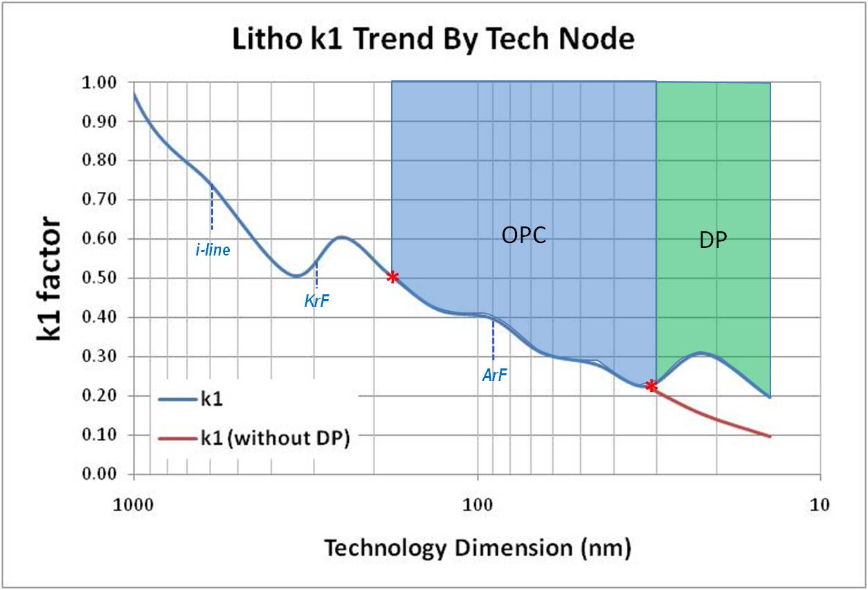
Figure 1: Litho k1 trend by technology node
EDA software came to the rescue at this point, by providing optical process control (OPC) technology to manipulate the layout in such a way that the process lithography tools could be “tricked” into printing what the designer intended. This not only extended the use of some very expensive lithography tools, but because the adjustments were applied post-tapeout (during the mask preparation phase), the designer didn’t even have to know about them.
Below 28 nm, we are reaching another roadblock where the k1 is now falling below 0.25. The next-generation EUV lithography tools are not yet ready for production, and the existing OPC software solution cannot, by itself, image the needed geometries. However, just like before, EDA software is coming to the rescue. A new technique of splitting the layout into two separate masks allows us to relax the layout pitch back into a k1 value that can be imaged with existing OPC solutions. This time, though, there is one big difference.
Unlike the introduction of OPC, which did not require the designer to be involved, this new double patterning (DP) solution will impose new layout, physical verification, and debug requirements on the designer. Figure 2 provides examples of several types of double patterning processes that may eventually be used at 22 nm and below. LELE (litho-etch-litho-etch) is the most common form of DP showing up at 22 nm. This technique also may allow a variation in which the original drawn polygons can be cut into pieces and stitched (overlapped at their cut locations) to facilitate more decomposition alternatives. SADP (Spacer-Assisted-Double-Patterning or Self-Aligned-Double-Patterning) utilizes a very different technique in the fab, and has a much more intricate mask decomposition requirement. The images illustrate how each technique is used to decompose (split) the original drawn layout into two new layers (dark blue and light blue), either automatically by the EDA software or manually by the designer. They also display examples of DRC violations caused by layout conditions that inhibited a successful decomposition.

Figure 2: Types of double patterning layout decomposition, and error checking
These new design requirements will require significant education of the design community, as well as significant new design implementation, verification, and mask generation software solutions from the EDA community. So, if you are a designer and you hear double patterning coming your way, it is best that you do a double take and pay close attention, or you may end up with double, double, toil and trouble…
 |
|
 |
|
 |
 |
 | |
 |
 |
Leave a Reply