Predicting the maximum allowable current density or lifetime in specific field conditions.

The downsizing trend of devices gives rise to continuous demands of increasing input/output (I/O) and circuit density, and these needs encourage the development of a High-Density Fan-Out (HDFO) package with fine copper (Cu) redistribution layer (RDL). For mobile and networking application with high performance, HDFO is an emerging solution because aggressive design rules can be applied to HDFO compared to the other package types such as Wafer Level Fan-Out (WLFO). HDFO allows assembly of more than one chip in one package and mostly fine Cu RDL is used to interconnect the chips. In addition, HDFO can be made in wafer and substrate level depending on the application, which has better scalability in terms of package size.
The Cu RDL in HDFO is embedded with a dielectric layer like polyimide (PI) and transfers the signal between chips or from the substrate to the chip. As current flows through the Cu RDL, heat is accumulated in the conductor due to Joule heating generation. This accumulation of heat can cause performance degradation. As the required current density and Joule heating temperature is increasing in the fine Cu RDL structure, it is regarded as an important factor on HDFO packaging performance.
Since the fine Cu RDL should have high reliability performance, various structures of RDL were introduced recently, such as embedded trace RDL (ETR) and Cu trace covered with inorganic dielectric for high density interconnection and reliability performance [1, 2]. Many studies regarding evaluation of fine Cu RDL reliability performance have been conducted, too.
Electromigration (EM) is one of the items to evaluate Cu RDL’s reliability and electrical characteristic performance. EM is a diffusion-controlled mechanism by gradual movement of the metal atoms in the conductor as a result of electron flow. This mass transport of metal atoms leads to the formation of voids on the cathode side and hillock on the anode side of the conductor. These processes result in the loss of electrical continuity. Electromigration behavior is affected by the feature size, stress condition, electron flow direction and test structure such as joint metallurgy. In case of Cu RDL EM testing, there is not only electron flow force but also thermal gradient in the conductor, so EM degradation is attributed to electrical potential and thermal energy [3].
Using EM test results, it is possible to predict the maximum allowable current density or lifetime in specific field conditions. EM tests performed under accelerated conditions and extrapolation based on the EM experimental data can be used to estimate the current or lifetime values of a use case. For calculation, Black’s model, which was published by James Black in 1969, is widely used. Some factors in this model are determined by fitting the failure distribution model such as Weibull and lognormal distribution. In this paper, EM characterization and failure analysis results of Cu RDL with ≤ 10 µm in an HDFO package under various current and temperature conditions is described. In addition, the increased ratio of estimated maximum allowable current under the several use conditions of operating temperature and lifetime is provided.
An HDFO package was made for Cu RDL EM testing. The package body and die size was 8.5 mm x 8.5 mm and 5.6 mm x 5.6 mm, respectively. The HDFO TV has a multi-layer RDL structure which has three layers of 3-µm thickness and Ti/Cu seed layer for each RDL. Also, polyimide was applied as a dielectric material surrounding fine Cu RDL. Above the RDL structure there are Cu pillar bump, die and mold. The mold type is over mold covering the die top side. The overall Cu RDL structure is shown in figure 1.

Fig. 1: Cross section view of HDFO test vehicle with its three RDLs.
A straight Cu RDL with 1000-µm length, 2- and 10-µm width was designed and tested. The Cu RDL was the most bottom layer (RDL3) in the HDFO. Four ball grid array (BGA) balls were connected to the tested Cu RDL for current forcing and voltage sensing. Figure 2 shows schematic illustration of the tested RDL design.

Fig. 2: Cu RDL design for electromigration test. ‘F’ and ‘S’ mean current forcing and voltage sensing, respectively.
The HDFO test vehicle was surface mounted to the test board for electrical connection with the EM test system and the second underfill was not applied after surface mounting. The 10-µm width Cu RDL was stressed under direct current of 7.5, 10 and 12.5 x 10⁵A/cm2 and temperature of 174, 179, 188 and 194°C. The 2-µm width Cu RDL EM test was also tested under direct current 12.5 x 10⁵A/cm2 and temperature of 157°C. The test conditions are indicated in table 1. The test temperature is considered to be the temperature at the Cu RDL. Therefore, oven temperature was set by compensating the amount of Joule heating. Joule heating calibration was carried out at each stress current because it depends on the amount of current density.
For calibration of the Joule heating, the resistance was measured at multiple temperatures under low and stress current conditions. The low current is regarded as the condition that generates non-Joule heating. The resistance value increases as the ambient temperature increases and the resistance change behavior at low current conditions is used to obtain the thermal coefficient of resistance (TCR) value. After the resistance measurement at a few temperature conditions, the amount of Joule heating was calculated using TCR and the resistance difference between low and test current condition. The calculated Joule heating temperature of each test current condition and the temperature at Cu RDL of 10-µm width are indicated in table 2.

Table 1: The fine-line Cu RDL EM test conditions.

Table 2: Joule heating temperature and temperature at rdl. Four test conditions were conducted for fine Cu RDL EM test.
The EM test continued until the resistance increased by 100% and the criterion to determine the time to failure (TTF) for calculating maximum allowable current was set to 20% resistance increase. The criterion of percentage increase in resistance is known to be most effective if all structures show very similar initial resistance. The initial resistance under the stress condition was 0.7 to 0.8 ohm for 10-µm width Cu RDL, so the values looked quite similar to each other. During the EM test, the resistance of the Cu RDL was measured using 4-point measurement technique. The number of test samples was determined to be 18 to 20 for meaningful statistical analysis.
In addition to an optical microscope, focused ion beam (FIB)/field emission scanning electron microscopy (FESEM) were used for failure analysis to understand of the degradation during the electromigration test. In addition to top view image analysis, specific areas were cross-sectioned by gallium (Ga) ion milling to observe the reduction of Cu RDL area by Cu oxidation and voids.
The resistance increase behavior of 10-µm width Cu RDL during EM test is shown in figure 3. The resistance increase trend can be divided into two different modes. In the early stage, the resistance increased steadily, but after reaching a certain resistance increase %, the resistance change occurred rapidly. The reason for the two stages of resistance increase is that the failure modes which occur dominantly are different at each step.
The different lifetime by temperature condition and time to failure (TTF) distribution under the same test conditions are also indicated in figure 3. It was estimated that the reason for distribution in TTF under the same conditions was due to different grain size of each Cu RDL among the test vehicles. The diffusion paths for Cu metal atoms are grain boundaries, material interface and bulk metal, and the activation energies of each diffusion path are different. Since the activation energy of grain boundary or material interface is lower than that of the bulk metal, the diffusion through grain boundary or material interface is more dominant during EM. Therefore, the grain size is an important factor which determines the TTF during EM tests [4].
In case of the lower current density of 7.5A/cm2, most of the samples showed a lower resistance increase and smoother curve compared to the high current 12.5A/cm2 as shown in figure 3 (c). Based on the results, it was expected that this low current condition could have a less severe failure mode than the high current condition, but the failure mode did not look significantly different between the high- and low-current conditions. In a further study, it is planned to do failure analysis with respect to the steps of resistance change behavior.
Additional EM testing was conducted with 2-µm width Cu RDL under the same current density condition (12.5×10⁵A/cm2) as 10-µm width Cu RDL and lower temperature conditions. The plotting of resistance increase during EM testing is presented in figure 4. In this case, the resistance change behavior showed only steadily increased resistance even in the long test time up to 10 Khrs, which was different from 10-µm width Cu RDL case. Based on the different resistance change behavior between low and high temperature conditions, it was suspected that the failure modes at high and low temperature were not identical. Also, it is expected that the failure mode of 2-µm width Cu RDL mainly occurred due to the steadily increasing resistance stage.
For 10-µm width Cu RDL, the number of units satisfying the failure criteria of 20% and 100% resistance increase are shown in table 3. All tested units satisfied the failure criteria of 20% within 8,000 hrs and some units showed under the 100% resistance increase when the test time was 10,000 hrs. Since the number of failure units was sufficient to do statistical analysis, the EM test was discontinued at 10,000 hrs. Also, the EM data where the resistance increased by 100% is secured so it is possible to calculate the maximum current capacity depending on the various failure criteria.

Fig. 3: Resistance increase behavior during EM test of 10–µm width RDL, 12.5A/cm2 current and (a) at 174°C and (b) 194°C temperature and (c) 7.5A/cm2 and 188°C.

Fig. 4: Resistance increase behavior during EM test of 2-µm width RDL. The test conditions were current density of 12.5A/cm2 and temperature of 157°C.

Table 3: The number of failed units of 10-µm width Cu RDL for each condition.
To understand the failure mechanism of the fine Cu RDL EM test, an optical microscope and FIB/FESEM were used to observe the top and cross-sectioned view. Figure 5 shows the 2-µm and 10-µm width of the Cu RDL after surface mounting on the test board. The thickness and width were well matched with design values and there was no abnormalities such as uneven surface, voids and delamination between Cu and PI at Cu RDL. As shown in figure 5, it was confirmed that the grain size in the RDL varied. Since the defects can influence the electromigration performance, the quality of Cu RDL should be checked before the EM test.

Fig. 5: FIB/FESEM image of Cu RDL after surface mounting: (a) 10-µm and (b) 2-µm width.
In the case of the 10-µm width Cu RDL, various failure modes were observed as presented in figure 6. First, delamination and Cu oxide were observed between the Cu RDL and passivation, which led to reduction of Cu RDL area and mainly attributed to the resistance increase. The reduction of Cu RDL area also resulted in the current crowding and higher temperature on RDL and EM degradation also accelerated. During EM testing, the voids were generated due to migration of Cu atoms and the delamination seemed to result from the voids growth along the interface between passivation and Cu RDL. The current density exponent value reflects which phenomenon is more dominant between void nucleation and growth. [5] Regarding the Cu oxide layer and diffusion into PI, Cu diffusion seemed to be accelerated due to electron flow or/and thermal gradient because at RDL2 (not EM tested), there is no oxide layer on the Ti/Cu seed layer to act as a barrier layer as shown in figure 6 (b).
Between Cu RDL2 and PI, only voids and Cu oxide layer were observed, which are due to thermal stress. In other words, the failure mode observed at the Cu RDL2 can be regarded as one of high-temperature storage (HTS) for a long time.

Fig. 6: Optical microscope and FIB/FESEM image of 10-µm width Cu RDL after test at 12.5×10⁵A/cm2, 174°C: (a) Cu oxide and delamination at tested RDL3 and (b) no Cu oxidation on the Ti/Cu seed layer at RDL2 (not EM tested).
Unlike the 10-µm width Cu RDL, the 2-µm width Cu RDL did not show the delamination between Cu RDL and PI, as figure 7 shows. From the less damaged 2-µm width Cu RDL, it is suspected that the growth of void along the interface between Cu RDL and PI resulted in the delamination shown in the 10-µm width Cu RDL. In addition, it was considered that this delamination could be a mainly contributing factor to the second stage showing resistance increase abruptly. It is planned to conduct a study for 2-µm Cu RDL electromigration under the higher current condition for comparison of the failure mode and parameter values in Black’s equation with 10-µm Cu RDL electromigration results. Also, it is expected to determine the failure mode of each resistance increase step through this further study.

Fig. 7: Optical microscope and FIB/FESEM image of 2-µm width Cu RDL after test at 12.5×10⁵A/cm2, 157°C: (a) Cu oxide void at RDL3 and (b) different FIB milling axis on Cu RDL3.
To predict the amount of Joule heating and failure locations, the electrical-thermal simulation was performed for 10-µm width Cu RDL. When the amount of heat accumulation is different in a Cu trace, the failure severity could be different by location because the EM damage is due to not only electron flow force but also a thermal gradient. As presented in figure 8, the actual test design and structure of the HDFO TV and test board were reflected in a simulation model, and the effective thermal conductivity of each structure was also applied. Table 4 shows a design of experiments (DOE) based on the oven temperature and sourcing current. The oven temperature can be regarded as an ambient temperature and the Joule heating amount is expected to vary with the sourcing current. The Joule heating simulation results are indicated in figure 9. The difference of Joule heating amount between the simulation and experimental value was 1.3 to 4.2°C, and the values of the two were almost similar. Also, the location showing the highest local temperature was the middle of the Cu RDL where the metal pads are connected, which was well matched with actual failure locations after EM test. To summarize, the Joule heating simulation results were well matched with actual EM test results in terms of Joule heating amount and failure locations, which was helpful to understand the EM degradation of Cu RDL and predict the failure locations.
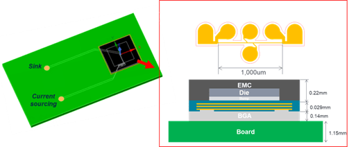
Fig. 8: Joule heating simulation model for 10-µm width Cu RDL.

Table 4: DOE for Joule heating simulation.

Fig. 9: Joule heating simulation results: (a) temperature contour and the point showing the highest temperature under the 12.5 x 10⁵A/cm2 and 137°C. (b) the Joule heating amount comparison between experiment and simulation.
For calculating the maximum current in field conditions, Black’s equation, which is related with time to failure in electromigration tests, is widely used.
MTTF = AJ-n exp (Ea/Kt) (1)
Where MTTF is the mean time to failure, A is the empirical constant, J is the current density, n is the current density exponent, Ea is the activation energy (eV), K is Boltzmann’s constant (8.62×10⁻⁵ eV/K) and T is the temperature (K). For determining the parameter of Black’s equation such as A, n and Ea, statistical analysis should be carried out first. It is very important because an extrapolation to a lower failure percentage based on the statistical analysis results is used for estimating current carrying capacity. Two typical methods to describe the EM failure distribution are Weibull and lognormal plots. The lognormal distribution is preferred when analyzing the failure of metal line and vias, whereas the Weibull model is usually used when the test structure has many independent elements which can cause the failure such as a bump and BGA ball electromigration. [6] Since the choice of fitting model could be critical when estimating the maximum current in a use case, a study regarding the distribution model in electromigration has been also performed [7]. In this study, a lognormal distribution was selected as a fitting model and the lognormal distribution chart of 10-µm width Cu RDL is shown in figure 10.
The maximum current carrying capacity was calculated under the assumptions that the failure mode is the same between this test and the use case, and Black’s equation is valid for both accelerated test and field conditions. The maximum current capacity in use case was estimated using Equation 2. In this case, the failure rate was assumed as 0.1% and the value of 3.09 came from the Z score of standard lognormal distribution.
J = [A exp (Ea/KT – 3.09σ)/TTF]-n (2)
Where T is temperature of use condition and TTF is the expected lifetime in the use case. For 10-µm width Cu RDL, Ea and n were determined as 0.74 and 1.88, respectively. In general, values of the activation energy and current density exponent are known as 1 and 2, respectively. In addition, the current density exponent value of 2 and 1 are generally regarded as void nucleation-controlled and growth-controlled, respectively. In this EM test, the failure mechanism appeared to be a mix of void nucleation and growth, and more specifically, the void nucleation appeared to be more dominant. If the failure mechanism is not same as this study due to some reasons such as severe test condition or different test structure, the estimated value could be different. Usually, the current density exponent (n) value increases when the over-stressed condition accelerates the EM degradation with Joule heating.
Table 5 shows the increase ratio of estimated maximum allowable current compared to the value under the field conditions which is a lifetime of 100,000 hrs, 100% duty cycle and a failure rate of 0.1%. The reference value for comparison is 10-µm width at 125°C, which is set as 1. When the operating temperature is decreased from 125°C to 110°C, the estimated current capacity was increased by 1.6 and 2.4 for 10- and 15-µm width, respectively. The failure criteria affect the value of maximum allowable current, so it is important to select the maximum current capacity for a design. As Equation (2) indicated, the maximum current increases exponentially – not proportional to the operating temperature. When this current estimation value is used for trace design, it should be also considered with the RDL fusing current because there is a cross point between calculated maximum allowable current and actual fusing current.

Fig. 10: Lognormal distribution for failure probability plotting of 10-µm width Cu RDL.

Table 5: The maximum allowable current (mA) ratio at several field conditions. The value of 10-µm width at 125°C is set as 1.
The electromigration behavior and failure mode of fine-line Cu RDL for high-density fan-out package was reported in this study. The tested width of Cu RDL were 2- and 10-µm, and the resistance increase due to degradation by electromigration was different for each test condition. In the case of 10-µm width Cu RDL, there were two stages showing different resistances change behavior. In the first step, the resistance steadily increased and void nucleation and growth were expected as the mainly occurred phenomenon at the first stage. The second step is a section where the resistance increased rapidly. This stage was only shown in the 10-µm width Cu RDL case, which showed delamination between Cu RDL and PI different from the 2-µm width RDL tested with low temperature and only showed Cu oxide and voids. Therefore, it was concluded that this delamination due to void growth is a major factor that affects to the resistance increase at the second step.
The observed failure mode after electromigration was Cu area reduction due to Cu oxidation and generation/growth of voids. Because the Cu migration into PI was also observed, it seemed to be accelerated due to electron flow or/and thermal gradient. Since a thermal degradation of PI should be considered in the Cu RDL EM test, an electrical-thermal simulation was performed to predict the weak position which is easily damaged and the results were well matched with actual test results. In addition, the Joule heating amount obtained by simulation was almost similar to the actual experimental values.
Based on the 10-µm width Cu RDL EM results, Black’s equation was completed so that the maximum current carrying capacity can be calculated. The lognormal distribution was used for statistical analysis with the calculated value of Ea and current density exponents were 0.74 and 1.88, respectively. The maximum current estimated under field conditions can be useful to design the RDL, but there are some considerations such as actual fusing current value and the dependency of Ea and current density exponent on failure mode and test conditions.
This research was supported by the Amkor Technology Global R&D center. The authors would like to thank to R&D Process/Material Research team for high-density fan-out TV preparation. Also, thanks to the colleagues of the R&D lab who cooperated for DUT preparation and failure analysis.
 |
|
 |
|
 |
 |
 | |
 |
 |
This is a remarkable clear explanation of the problem of measuring temperature time relations at the chip
Level
Let’s try and work further with our companies here