The switch to transformer models has increased AI-driven computing demand by a factor of 50 million over five years.

As artificial intelligence (AI) proliferates rapidly, AI models and datasets are also growing rapidly in size. This growth far outpaces performance improvement in hardware systems, and is increasing AI’s energy consumption unsustainably.
To address these challenges and explore collaborative solutions, SEMI’s Smart Data-AI Initiative – as part of its Future of Computing focus – recently hosted a day-long workshop on Sustainable AI Systems that brought together domain experts from the entire AI ecosystem. Speakers included industry leaders Applied Materials, AMD, Arm, ASE, Google DeepMind, IBM, Intel, Lam Research, McKinsey, Micron, NVIDIA, Qualcomm, SK hynix; exciting start-ups Cerebras, LightMatter, Mentium Technologies and Mueon; and leading-edge academic institutions, Stanford University and University of California, Davis & Irvine. The keynotes, panels and spirited audience discussions covered novel devices, materials, advanced packaging, chiplets, photonics and architectures & algorithms for data centers, cloud and edge. This article synthesizes high-level insights from the workshop.
The day started with a basic question: Why is AI essential to continued progress and prosperity? The answer lies partly in shifting global demographics, with the population aging in most developed economies. At the turn of the century, there were ~6 people in the workforce supporting each retiree, but projections indicate there will be only 2 active workers per retiree by 2050. In parallel, productivity growth rates have fallen to half of what is required. AI can help bridge this gap, if we can ensure continued progress of AI in a responsible and sustainable manner.
A formidable roadblock to continued progress of AI is its rising energy demands. For example, the energy used by some large language models (LLMs) to run just one training cycle could be used to power thousands of homes. The switch to transformer models has increased AI-driven computing demand by a factor of 50 million over 5 years, and by some projections, this demand will consume half the world’s generation capacity by 2050. This is clearly not sustainable! All players in the ecosystem are deeply committed to reducing AI’s energy consumption, and the industry has already decreased the energy used per token of computing by a factor of 100K in the past 10 years. However, the rapid growth of AI outpaces this, highlighting the huge challenge ahead.

This workshop was developed with the hypothesis that innovation is required across all segments, and an important first step is to initiate a dialogue. Our highly distinguished speakers covered the entire solution stack, and while it is impossible to capture the ocean of insights that they shared, the following provides a flavor.
Materials and devices used to build semiconductor chips form the foundation of the stack for all computing systems. Silicon substrates with copper interconnects remain industry’s mainstay, but are being augmented by innovative ideas.
As device dimensions continue to shrink, novel 2D materials such as MoSe2, WSe2, ZrSe2 and NbP are being researched. While Si mobility degrades with decreasing film thickness, 2D materials maintain high electron mobility in thin-film substrates. These can be stacked to build 3D systems with lower power consumption than traditional planar structures. In parallel, novel device technologies such as gate-all-around (GAA) can provide power savings up to 25%.

These novel materials and devices are complex, and require almost magical wizardry to build. For example, they may require depositing a stack of multiple defect-free films that are only a single (or few) atomic layer(s) thick, or etching a steep well that is one hundred times as deep as it is wide. It is an incredible accomplishment of the semiconductor industry to build these devices and chips successfully, but it is getting harder and more expensive. Consequently, AI is now being used as a tool to help with the ever-growing fabrication complexity of semiconductor R&D and manufacturing. This is a synergistic virtuous cycle, where AI algorithms enabled by chips are used in turn to help with chip fabrication.
The next layer of the stack is the integration of individual devices into a system. Advanced packaging techniques, such as silicon or glass interposers (2.5D) for interconnecting chips, can reduce the communication distance and power consumption. These are often deployed for high-performance computing systems running AI algorithms. Beyond this, the industry is actively exploring 3D systems that are even more compact, both as multi-die 3D packages and as monolithic 3D chips.
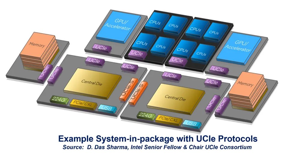
The concept of chiplets – smaller chips with specialized functions that can be assembled flexibly to optimize system performance – holds much promise. Industry consortia are developing protocols such as Universal Chiplet Interconnect Express (UCIe) to enable seamless integration of chiplets both in the planar and vertical dimensions.
These advanced techniques pack more functional elements into increasingly compact form factors, but this proximity makes power delivery challenging and often generates intense heat. Much work is needed to ensure optimal power delivery and adequate thermal dissipation.
Looking beyond traditional electronics, photonics represents an exciting opportunity. Most long-distance data communication is on fiber-optic cables and thus already photonic – bringing this to shorter distances can save energy while increasing bandwidth and performance. This requires efficient photonic-electronic integration at the packaging or even chip level, which is a major challenge requiring cross-disciplinary collaboration.
AI algorithms need enormous amounts of data processing compared to traditional computing workloads. This requirement stretches (or breaks) the limits of traditional Von Neumann architecture, which requires frequent data movement between memory and processor elements for each computation cycle.
Much of current architecture innovation focuses on bringing processor and memory elements closer to each other. System integration is already driving “compute-near-memory” architectures like high bandwidth memory (HBM). Other forward-looking implementations combine them into a single chip, known as compute-in-memory (CIM). Memory elements being explored for this purpose include resistive RAM (RRAM), phase-change memory (PCM), ferroelectric RAM (FeRAM) and magnetic RAM (MRAM). However, there is no one “perfect” memory – each has pros and cons in terms of latency, capacity, bandwidth, power consumed per operation, manufacturability, etc. Other researchers are also exploring devices like memristors for analog computing, which can improve energy efficiency for certain workloads.
Finally, hardware-software co-optimization is crucial. Algorithms mismatched with the underlying system are energy expensive; conversely, co-optimized systems are highly efficient. While conceptually obvious, this is difficult in practice because development cycles are quite different – software algorithms can transform in a few months, while new hardware often takes years to develop. While some strategies can be used for mitigation – such as designing in redundancy/flexibility or making the hardware application-specific – much work remains to solve this conundrum.
All speakers emphasized that pre-competitive collaboration across the entire stack is critical, as these challenges are formidable and cannot be solved by one entity or in isolated silos. SEMI is a global and neutral organization with over 3,000 member companies, and is well-positioned to provide a pre-competitive collaboration platform to connect the dots across silos. In fact, SEMI’s mantra is “Connect, Collaborate, Innovate” – reinforcing its commitment to advancing the entire industry. For this purpose, SEMI’s Smart Data-AI Initiative continues to drive robust discussions on this topic – next there will be a roundtable discussion during SEMICON Southeast Asia, May 20-22 in Singapore, followed by a focused technology session at SEMICON West 2025, October 7-9 in Phoenix, Arizona.
The overall objective is to move from “talking-the-talk” to “walking-the-walk,” towards creating system-level solutions for energy-efficient AI computing. Specifically, we want to identify the pre-competitive actions that could synergize individual innovations and make the whole greater than the sum of parts. Some ideas include collaborative proof-of-concept projects, industry standards and independent benchmarking. Come join us on this journey and connect with us at [email protected].
 |
 |
 |
|
 |
 |
 |  |
Leave a Reply