AI-driven design benefits projects at mature nodes, too.

Over the last few years, artificial Intelligence (AI) has increasingly played a significant role in the chip development process. But, when people talk about AI-designed chips, it is usually in the context of the latest, cutting-edge designs manufactured at advanced process nodes (7/5nm and smaller) and for good reason. Such designs constantly push the bounds of power, performance, and area (PPA) amid stringent manufacturing rules. They rely on weeks or even months of experiments led by experienced engineering resources to craft the best results possible. This approach, commonly known as design space exploration (DSE), comes at a huge cost of designer productivity and time to market while still leaving PPA on the table. The need for a smarter and efficient way forward for chip design is clear which explains the rapid adoption of AI-enabled tools and solutions.
AI-driven design applications are proving to be a huge boon to the semiconductor industry. They enable designers to achieve solutions previously thought impossible and, in many cases, unattainable by traditional methods. As the saying goes, “the proof is in the pudding.” From the recent article in WIRED magazine describing how Samsung leveraged Synopsys AI software to design their latest Exynos smartphone chips to several real-world results presented by Aart de Geus, the chairman and co-CEO of Synopsys, in the recent Hot Chips conference keynote address, the results of applying AI to design industry’s cutting-edge, advanced node chips are impressive.
However, is there value in applying AI to every design? What about “well established” designs at more mature process nodes? The answer is a resounding “Yes!” and it is an extremely important one too. Let us take a closer look.
The majority of electronic applications today across home appliances, computers, automobiles, mobile, industrial equipment, and healthcare have at least few chips at mature process nodes (16/14/12nm and larger). In fact, such designs account for more than 50% of chips being designed today and the trend continues in the future, as shown in a recent IBS report.
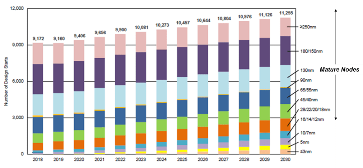
Fig. 1: Design start trends. (Source: Design Activities and Strategic Implications, IBS 2021)
With a strong demand for chips at mature nodes, designers face several challenges in evolving these devices to meet changing demands. For example, most electronic products are under increasing cost pressure over time, so there’s an incentive to reduce the die size of devices as much as possible. Although performance is usually not a top priority for these chips, more speed may be required when new competitive products appear. Similarly, new features may need to be added in response to competition or to address varying market applications, and usually it’s not acceptable to increase area, cost, or power. Adding to all these challenges is the continuing global chip shortage, worsened by the pandemic and supply chain issues which may require switching supplier and redesigning.
Migrating to a smaller node to add features, shrink die size, or lower power for a new or derivative design is not always an option, both for cost reasons and because the effort involved can be considerable. Most analog circuitry must be redesigned and cannot simply be scaled. Even re-targeting digital logic to a newer node or different supplier is labor-intensive, requiring significant experimentation to tune design flows for best results. Given that mainstream designs in mass production tend to have fewer engineering resources available, node migration adds considerable risk to a project schedule.
This is where AI-driven automation can help address the growing demand for differentiated products while allowing design teams to focus on the innovation pipeline (Synopsys’ DSO.ai – Design Space Optimization AI – is such a solution for AI-driven chip design). Using reinforcement leaning technology to autonomously search the vast chip design space for optimal solutions, an AI assistant can help engineers build better, faster, and cheaper semiconductors.
A recent customer presentation at a Synopsys Users Group (SNUG) event showcased the benefit of AI-driven design solution on multiple 40nm production chips. The four designs described were in the 5-10 million gate range running at 100-200MHz—mainstream by today’s standards. The key objective for the customer was to reduce power and area for their next generation products with minimal turnaround time and fewer engineering resources.
On the first design, an expert-level engineer had worked for a month to fine tune and optimize the design to reduce power consumption by 9%. Applying the Synopsys AI solution, in just one week the design team had a solution with 12% power savings. With no prior training data (cold start), AI beat the expert engineer generated results by 3% in a quarter of the time, using fewer resources.
Since DSO.ai has a learning system that continuously trains and updates its machine-learning models, reuse across designs and projects helps organizations scale to AI-grade productivity. For the second design, the customer applied this learning system (warm start) throughout the design cycle across varying revisions, achieving 7% power reduction, a target previously considered unattainable.
Encouraged by these positive results, the AI solution was applied to help optimize area for two more production designs. In the first of these, the customer achieved 4.4% area savings. Taking it one step further, learnings from this design were re-used for a subsequent, derivative design. This cross-training resulted in an area reduction of 12% with almost no human interference–unleashing the true power of AI for chip design.

Fig. 2: AI results for four 40 nm projects. (Source: Synopsys)
AI has tremendous potential to improve many aspects of chip development: logic design, implementation, verification, validation, test and more. We are just at beginning of what will be a new era of AI-driven design. With the recent resurgence in hardware demand across every market segment, it is fortunate we have AI helping us accelerate chip design at every node.
 |
|
 |
 |
 |  |
 |  |
Leave a Reply