Testing every configuration of a package in a lab is practically infeasible, but thermal simulation can help.

By Prasad Tota and Robert Day
Throughout the electronics industry, submicron feature size at the die level are driving package component sizes down to the design-rule level of the early technologies. Today’s integrated circuit (IC) package technology must deliver higher lead counts, reduced lead pitch, minimum footprint area, and significant volume reduction, which has led to semiconductor manufacturers developing the small outline package (SOP), surface-mount memory packaging.
SOP packages support the trend toward miniaturization by consuming one-third to one-half the volume of earlier packaging alternatives. SOP components are a logical choice for the small form factor of handheld instruments, portable communication devices, laptop and notebook PCs, disk drives, and numerous other applications. The mechanical dimensions of the power SOP (PSOP) package, combined with a heat spreading thermal mass (copper slug), make it a good choice for office automation, industrial controls, networking, and consumer applications that generate internal heat and are exposed to stressful temperature conditions.
The PSOP leads are located on the long side of the package, which leaves two sides of the package open. The open sides of the package can be used to route traces under the component, conserving board layers and simplifying board layout. Compared to older versions, the packages can be placed much closer to each other and to other components on the board.
When IC packages are downsized, thermal power density increases, and the heat-transfer path from the die to the external ambient needs to be optimized to allow for maximum possible power dissipation at the die while still ensuring the die temperature is under the maximum allowable value.
Although PSOP undergo tests for reliability under temperature stresses, electrical flow, and solderability, as well as mechanical inspection at the manufacturer before shipping, it would be time-consuming and expensive to physically test or design test boards to test a package in all its possible applications and configurations.
Computational fluid dynamics (CFD) software is useful in such situations because it can simulate and estimate the junction temperature (Tj) of the IC when attached to the PCB under various conditions, including different powering conditions, board conductivity, thermal via distribution, bill of materials, and the IC package construction itself. CFD tools enable a mechanical or electrical engineer and/or IC designer to quickly see the effect of design changes from a thermal management perspective both qualitatively and quantitatively.
To test this, we used FloTHERM to perform computational thermal analysis of an Analog Devices high-speed, high-voltage, 1-A output drive amplifier, the ADA4870-1, PSOP mounted on a PCB [1]. Specifically, we wanted to identify the maximum power that could be dissipated on the die active area while keeping the Tj at less than 150 °C. We studied various environments to estimate this maximum power, for example, changing the board area, adding thermal vias, and attaching a heatsink.
This package can be surface-mounted on the board either slug down or slug up (Figure 1), depending on the direction of the formed leads. In a slug-down configuration, the component is surface-mounted on the primary side of the board where the copper slug is soldered to the top side of the board. In a slug-up configuration, the leads are soldered to the primary side of the board. For our experiment, we used a slug-down configuration; first with no heatsink, and then with a heatsink attached to the secondary side of the board with thermal grease between the board and the heatsink base.

Figure 1: The PSOP dimensions in millimeters, with the copper slug on the bottom.
For the CFD simulation, the test board we used was a six-layer board, with dimensions of 59 x 61 mm. We assumed that the copper coverage for each of the conducting layers was smeared uniformly within the layer’s volume. Based on this, we calculated the thermal conductivity (k) of each layer as a volume average based on the percent of copper coverage within an individual layer (Table 1). For further accuracy, we could also have processed the images for copper coverage within a layer to provide a conductivity mapping within the plane of the board [2].
Table 1: Board stack-up and percent of copper coverage.

We recommend discretely modeling each of the conducting layers with orthotropic conductivity for the entire thickness of the board to accurately predict the value of the junction temperature. Modeling the layers discretely, rather than with a lumped model, captures the effect of heat spreading within the board more accurately for various heat-transfer paths.
Thermal simulation without a heatsink
We conducted the first set of simulations to study the thermal behavior of the PSOP mounted on the primary side of the board where the copper slug was soldered to the board. We kept the board horizontal with respect to gravity in an ambient temperature of 85 °C.
To emulate real working conditions, we applied heat to two-thirds of the top of the die. In the simulation, the junction temperature (Tj) was measured at the geometric centroid of this area, and case temperature (Tc) was measured at a point in the copper slug just above the soldered interface (Figure 2). It is possible to also monitor the temperature of the leads, plastic surface, or any given position to validate the computational results with available test data.
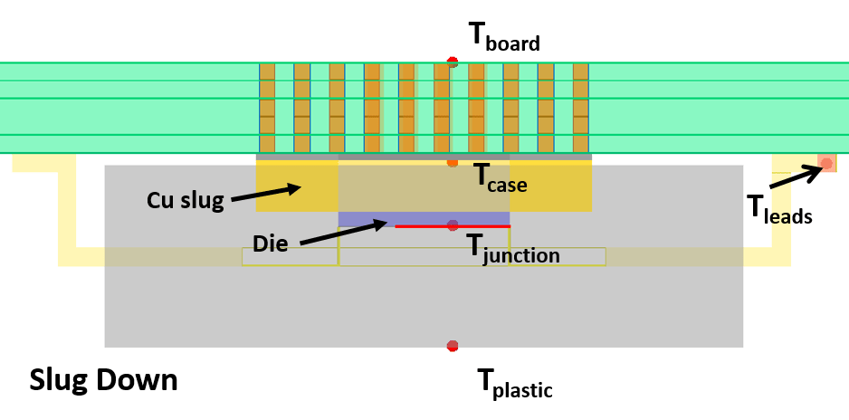
Figure 2: Temperature measurement locations.
We added thermal vias under the slug to provide a more conductive path from the copper slug into the board. The vias were placed right under the copper slug because our numerical investigations revealed a small advantage of adding vias beyond the slug area. This also helps in lowering the manufacturing cost of the board.
We investigated two possible scenarios for thermal vias: one where the inner layers were isolated, and a second where the inner layers were stitched together. Stitching the inner layers lowers the junction temperature because a fraction of the heat entering the slug can spread in inner layers; however, including the inner layers raises the core body temperature of the board. So depending on the application, the inner layers could be isolated or used for thermal management. In this study, the secondary side of the board was completely covered with copper.
Figure 3 shows the temperature plots for the package in still air at 85 °C and thermal power P = 2 W with die-attach material of k = 1.6 W/mK [watts per meter kelvin]). We replaced the die-attach with the more conductive material, k = 50 W/mK, which significantly reduced the junction-to-case thermal resistance (θjc) of the package from 6.61 °C/W (celsius per Watt) to 1.12 °C/W.

Figure 3: Temperature plots for the package in still air at 85 °C.
Thermal simulation with a heatsink
We soldered a heatsink to the back side of the board to increase the power dissipation through the package, using thermal grease between the board and heatsink. Adding the heatsink significantly reduced the junction-to-ambient thermal resistance (θja) from 16 °C/W to 5.73 °C/W. Heat-flux plots for a plane cutting through the package show the heat spreading over a larger surface area hence reducing the junction temperature for a given value of thermal power (Figure 4).

Figure 4: Heat-flux plots for a plane cutting through the package.
Table 2 shows the results for maximum power (Pmax) allowed in the slug-down configuration in still air with and without a heatsink for the two die-attach materials. Based on these results, we focused our next study with the more conductive die-attach material (Cookson).
Table 2: Thermal resistance for different die-attach materials.
| Slug-Down Configuration: Still Air at 85 °C | ||||
| Die Attach | θjc (C/W) | θja (C/W) | Pmax | |
| Without heatsink | Ablebond | 6.61 | 21 | 3.11 |
| Without heatsink | Cookson | 1.12 | 15.95 | 4.10 |
| With heatsink | Ablebond | 6.78 | 10.63 | 6.11 |
| With heatsink | Cookson | 1.11 | 5.73 | 11.34 |
We wanted to find the shortest heatsink sufficient to dissipate 10 W of heat at the die. We used the parametric study capability in the CFD software to quickly set up and solve for different scenarios [3]. The variable parameter in this case was the heatsink fin height. The results are shown in Figure 5; junction temperature (Tj) is represented by circles and case temperature (Tc) by squares. We found that a heatsink with fin height of 10.36 mm is sufficient to dissipate 10 W.

Figure 5: Junction temperature (Tj) and case temperature (Tc) for different heatsink fin heights.
These results prompted us to investigate further to find Pmax that could be dissipated if there were tighter constraints on the size of board and heatsink, and hence we reduced the size of both to 30 x 30 mm. We also studied the effect of different fin heights on junction-to-ambient thermal resistance, θja (Table 3).
Table 3: Thermal resistance vs fin height in still-air environment.
| Board and Heatsink Base: 30 x 30 mm | ||
| Fin Height (mm) | θja (C/W) | Pmax (W) |
| 21 | 11.82 | 5.50 |
| 15 | 12.98 | 5.01 |
| 10 | 14.48 | 4.49 |
| 5 | 17.12 | 3.80 |
With forced airflow, the junction-to-ambient thermal resistance could be further reduced, allowing higher powers to be dissipated and Tj to be kept under 150 °C. Figure 6 shows the package simulation in a forced-air environment. Table 4 shows the results for heatsink optimization in forced air. It is interesting to see that, with forced airflow of 2 m/s, the package could dissipate over 20 W of heat for a fin height of 21 mm and 17 W with fins just 10-mm high.

Figure 6: Package with heatsink in a forced-air environment.
Table 4: Thermal resistance versus fin height in forced air. θja: junction-to-ambient thermal resistance, Pmax: maximum power.
| Forced Air, Heatsink Base 61 x 59 mm | ||||
| 1 m/s | 2 m/s | |||
| θja | Pmax (W) | θja | Pmax (W) | |
| 21 mm | 3.59 | 18.1 | 3.18 | 20.4 |
| 15 mm | 3.95 | 16.5 | 3.42 | 19.0 |
| 10 mm | 4.46 | 14.6 | 3.8 | 17.1 |
| 5 mm | 5.36 | 12.1 | 4.49 | 14.5 |
We did a similar parametric study for the smaller heatsink with a base of 30 x 30 mm for different fin heights in forced air (Table 5). This smaller heatsink with 10-mm high fins (lower weight) offered the same performance as a larger heatsink with 5-mm fin height.
Table 5: Thermal resistance and maximum power for forced air. θja: junction-to-ambient thermal resistance, Pmax: maximum power.
| Forced Air, Heatsink Base 30 x 30 mm | ||||
| 1 m/s | 2 m/s | |||
| θja | Pmax (W) | θja | Pmax (W) | |
| 21 mm | 4.4 | 14.8 | 3.62 | 18.0 |
| 15 mm | 4.85 | 13.4 | 3.95 | 16.5 |
| 10 mm | 5.46 | 11.9 | 4.42 | 14.7 |
| 5 mm | 6.48 | 10.0 | 5.3 | 12.3 |
Several parameters effect the thermal conductivity of the board in the region of the vias [4]. Creating a test board for every possible thermal via configuration and testing in a lab is practically infeasible. The CFD tool can be used to perform sensitivity studies of thermal performance to various via parameters, such as the pitch, plating thickness, and fill material (Figure 6). Such computational studies reduce the number of prototypes needed for testing or validation.
In a CFD program, it is computationally intensive to model each and every via discretely, so we took a lumped approach where we replaced the region of vias with a block of orthotropic conductivity that had in-plane conductivity (kxy) and through-plane conductivity (kz). A board-import tool in the software was used to calculate the kxy and kz of this via block, but we could also have calculated these values analytically [2, 5].
Thermal vias with an outer diameter of 0.3 mm were studied. Figure 7 shows the sensitivity of thermal conductivity of via block to pitch and plating thickness (t). The dielectric material used in this calculation was FR4 (k = 0.3 W/mK), and the fill material was pure copper (k = 385 W/mK).
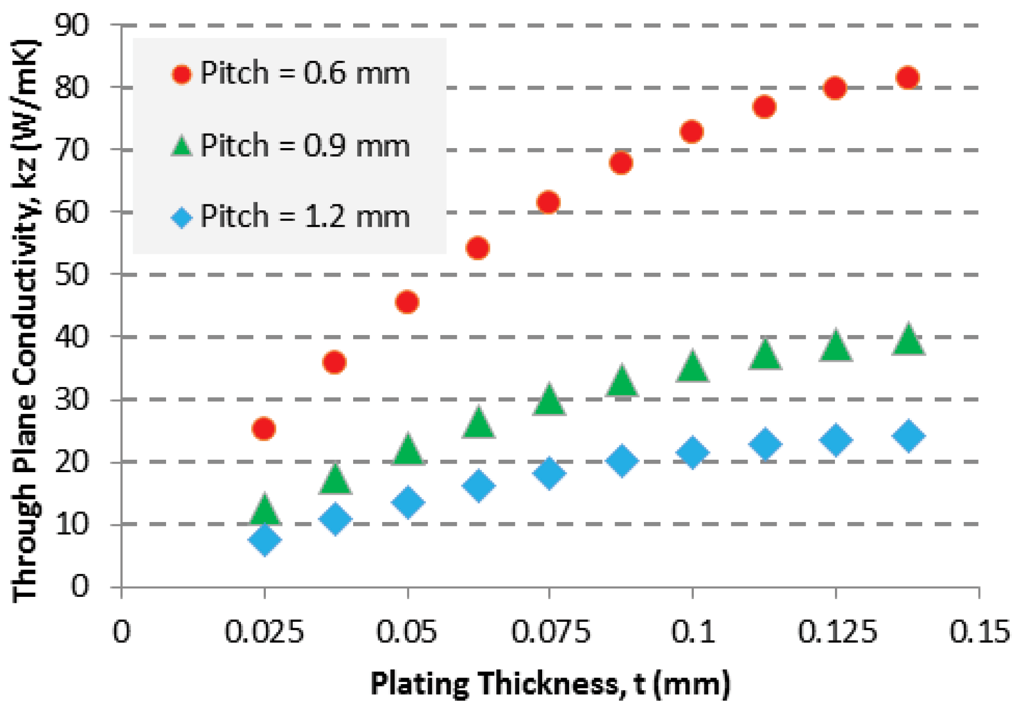
Figure 7: Sensitivity to via pitch and plating thickness. kz: in-plane conductivity.
Thermal simulations were conducted for PSOP in still air based on the conductivity values of the via cuboid, and results are shown in Figure 8. The results show that when plating thickness t is 75 µm or higher, even sparsely populated vias are sufficient. However, at low plating thickness, say 25 µm or lower, the vias need to be populated densely to ensure the component does not experience thermal failure.

Figure 8: Junction-to-ambient thermal resistance (θja) to via pitch and plating thickness in still air.
Validating the simulation results
We conducted lab experiments to validate the CFD model results. The IC inside the PSOP package is capable of dissipating 10 Watts of power and has an integrated temperature monitor. The relationship of the voltage at monitor-to-die temperature is not an absolute temperature indicator. However, the change in voltage versus temperature is a reliable indicator of relative changes in die temperature. Calibrating the temperature-monitor voltage versus temperature function was the first step in understanding die temperature used to determine thermal resistance.
The PCB we used in the lab was FR4-grade with six layers of copper and exposed copper planes, onto which the ADA4870-1 PSOP package was soldered and heatsinks were mounted. We used copper-filled thermal vias to conduct heat from the IC side to the bottom of the board where a precise temperature sensor was soldered directly below the thermal slug of the PSOP package onto the back side of the PCB. We bolted a heatsink to the back side that straddled the sensor using silicon grease as a thermal interface material between the heatsink and the PCB. We used commercially available heatsinks (Table 6).
Then, we placed the PSOP assembly into a still-air chamber using automated instruments and power supplies and allowed it to soak overnight without any power applied. The ADA4870-1 IC and temperature sensor were then both turned on and measurements of the PSOP temperature-monitor voltage and sensor-trimmed PTAT (power sub-threshold proportional to absolute temperature) current were made immediately. The temperature-monitor voltage measurement was related to the absolute temperature indicated by the temperature sensor. We repeated this process at several temperatures to develop a calibration of the temperature-monitor voltage to absolute temperature (Figure 9).

Figure 9: Temperature monitor (TM) volts versus sensor temperature.
Using a linear fit to the curve (T [°C] = TM [V] – 1.93/0.003), we converted the voltage to temperature. We conducted additional steady-state tests to reveal the practical limits of power dissipation (maximum power) as a function of the applied heatsink. As shown in Table 6, large heatsinks are necessary when operating at the limits of power dissipation for the tested IC. We calculated the junction-to-ambient thermal resistance () from the measured data by the following relationships at steady state: = Δ () − 1.93 () − 0.003 /° Δ () = °/.
Table 6: Thermal testing versus simulation results. θja: junction-to-ambient thermal resistance, Pmax: maximum power.
| Package Mounted in Slug-Down Configuration | ||||
| Test Data | CFD Data | |||
| Test Case | θja | Pmax (W) | θja | Pmax (W) |
| 25 °C no heatsink | 12 | 10.42 | 16 | 7.81 |
| 25 °C w/ VHS-45 | 7 | 17.86 | 8.87 | 14.1 |
| 85 °C no heatsink | 12 | 5.33 | 16 | 4.1 |
| 85 °C w/ VHS-45 | 7 | 9.14 | 7.81 | 8.35 |
| 85 °C w/ VHS-95 | 6.2 | 10 | 5.73 | 11.34 |
The results showed the CFD simulation to be in good agreement with the lab test results with a heatsink mounted, where the dominant heat-transfer path is from the die into the heatsink. There is a higher difference for simulations with no heatsink, where an appreciable fraction of the total heat travels through bond wires and leads into the top layer of the PCB. This difference can be attributed to assumptions in simulation we made in modeling the leads and bond wires in the simulation.
Conclusion
With these experiments, we found that CFD software is a complimentary tool to laboratory testing, enabling quick parametric and design optimization studies in the thermal design. Such data is useful for studying electronics in harsh environments with increasing demands on power. The next step would be to analyze the transient behavior of the package and thermal characterization using structure functions generated by hardware testing, such as the Mentor T3Ster. A transient thermal simulation validated by test data would go a long way in simulating the transient response of a package for various powering conditions and reduce the number of laboratory tests needed.
References
Robert Day is a senior engineer for high voltage linear applications at Analog Devices.
 |
|
 |
 |
 |
 |
Leave a Reply