The possibilities of what can be done are endless, but what does it mean for designers?

Ed Sperling’s June article New Approaches to Better Performance and Lower Power took a look at the new materials that researchers are examining for future technology nodes.

Figure 1. Basic Planar CMOS FET
Figure 1 shows a basic diagram of a planar CMOS FET (diagrams for other FETs can be found here). The drive strength of a FET is proportional to ![]() , where μ is the surface mobility for the majority carriers (holes or electrons) in the channel. This has led to transistors designers focusing on shrinking L(g), increasing C(ox) and increasing μ. Shrinking the gate length has historically been a large part of defining the next technology node, but that relationship has become a bit fuzzier as we push to ever decreasing feature sizes. Clearly this is dependent on the ability to reliably create very small feature sizes on a chip. C(ox) can be increased by decreasing the oxide thickness, which has run into atomic limits where being off by one layer of atoms can cause significant deltas in the drive strength of the transistors leading to more variability in the design. C(ox) also can be increased by improving the dielectric constant of the insulating material and this the “HK” in HKMG processes that use Hafnium Oxide to increase C(ox) but still have a thick enough insulating layer to prevent breakdown and control variability.
, where μ is the surface mobility for the majority carriers (holes or electrons) in the channel. This has led to transistors designers focusing on shrinking L(g), increasing C(ox) and increasing μ. Shrinking the gate length has historically been a large part of defining the next technology node, but that relationship has become a bit fuzzier as we push to ever decreasing feature sizes. Clearly this is dependent on the ability to reliably create very small feature sizes on a chip. C(ox) can be increased by decreasing the oxide thickness, which has run into atomic limits where being off by one layer of atoms can cause significant deltas in the drive strength of the transistors leading to more variability in the design. C(ox) also can be increased by improving the dielectric constant of the insulating material and this the “HK” in HKMG processes that use Hafnium Oxide to increase C(ox) but still have a thick enough insulating layer to prevent breakdown and control variability.
The other variable left in our equation is μ. Increasing surface mobility has been researched for years and transistor designers have looked to materials other than silicon (Si) to improve transistor performance. For reference purposes, Figure 2 shows a relevant section of the Periodic Table of Elements.
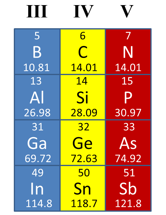
Figure 2. Elements of Interest in Series III, IV and V
Richard Stevenson looks at Changing the Transistor Channel in a recent issue of IEEE Spectrum. There is a veritable alphabet soup of III-V compounds like GaAs, InGaAs and InP mentioned that can help to improve the channel mobility of a FET. Transistor designers have also been using another IV series material, Ge, to produce strain to increase mobility. By mixing larger Ge atoms with Si in the source and drain regions of a transistor, the channel region is compressed and this increases the mobility of the channel in a PFET. (For readers interested in more detail, Nuo Xu’s dissertation performed at UC Berkeley has some great SEMs and diagrams.) Indium gallium arsenide (InGaAs) has an electron mobility that is greater than 6x that of silicon. With this type of jump in mobility it’s not surprising that researches would want to find ways to incorporate this material into their transistor structures. Going to a compressed channel made of germanium (using smaller silicon atoms underneath it to provide the compression) could yield a 6x increase in the hole mobility of the germanium in the channel.
There are challenges though in creating reliable structures using these compounds and a lot of the methods being researched involve creating linear trenches. Given the lithography challenges, it’s not too hard to imagine that the design rules will become even more restrictive going forward. What if at some point the only reliable structures that could be built would favor a fabric type of implementation? One large IDM, Intel, has in the past few years been in the press for helping to fund Tabula and making their 22nm process available to them. There has also been news about Intel providing fab services for Achronix and recently for Altera at 14nm. This might just be a way to help keep the alligators (fabs) fed or could it be a hedge in case the future just happens to look a little more fabric-like? Perhaps it is both.
So where does this all end up? How about the possibility of a transistor design based on a single atom of phosphorus?
 |
|
 |
 |
 |  |
 |  |
Leave a Reply