Finding failure sites that are hidden from optical view.

A typical semiconductor is fabricated from metal and barrier layers separated by passivation layers. A further glassivation and/or polyimide layer on top of these provides environmental and mechanical protection.
Optical microscopes
By using optical microscopy, the semiconductor die can be inspected for failure modes such as top-down visible crack degradation, melt-down of metal conductors, etc. However, if the failure site is hidden from optical view, or if characterisation of metallisation quality needs to be performed, the IC needs to be deprocessed to provide samples for analysis.
Deprocessing – layer by layer
DELTA can provide top-down deprocessing (delayering) of the whole die, exposing metal and passivation layers one by one for visual inspection by means of Scanning Electron Microscopy (SEM). This process also allows parts of the device that are not accessible from the bonding pads to be probed electrically, to support functional debugging.

Fig. 1: A die before and after deprocessing – all four metal layers are uncovered in one step.
Reactive ion etching (RIE)
Deprocessing is achieved typically by using a combination of plasma reactive ion etching (RIE) and wet chemical selective etching. The top passivation layer is removed by RIE. A suitable mixture of gases, pressure and RF settings is chosen based on the materials that need to be removed (which is typically a sandwich structure consisting of a polyimide layer on top of silicon nitride and/or silicon oxide).
Metal layers and subsequent barrier layers are then removed by dedicated selective wet chemical etching. Passivation inter layers are then again removed by the appropriate form of RIE.
SEM
After each deprocessing step, the semiconductor is inspected optically. For higher resolution, examination of very small structures like the microstructure of a failure site, sub-micron size conductors or evaluation of metal step coverage and/or metallisation voiding, SEM is the preferred analysis tool.
The images below illustrate typical SEM documentation of various stages of deprocessing, to show what can be investigated, and the ability of the technique in providing highly detailed views, measuring critical dimensions and evaluating processing quality:
Images of SEM documentation

Fig. 2: All four metal layers and poly layers are uncovered (12,000x magnification).

Fig. 3: A processed sample titled at 30º to provide a perspective view (6,000x magnification).

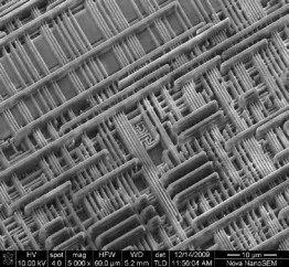
Fig. 4: Another part of the deprocessed sample titled at 45º (5,000x magnification).

Fig. 5: Enlargement of the bottom ‘Metal 1’ metal layer of a device, allowing grain boundaries to be examined (50,000x magnification).

Fig. 6: The top glassivation, metallisation and barrier layers have been removed on this sample (3,000x magnification)

Fig. 7: The passivation layer and the plugs connecting to the next metal layer can now be examined (8,409 magnification).
Leave a Reply