
Recently, we were invited to participate in an internal Chips@Cisco event along with other EDA vendors and FPGA providers. Executives from these vendors participated in a panel to discuss the challenges seen by the technology leaders in FPGAs and what it means to the industry. Everyone on the panel agreed that design size and complexity, including clock domains, is continuing to follow Moore’s law with no slowdown any time soon.
Increasing SoC design size and complexity is no surprise to anyone, but what is exciting is that the latest FPGAs using the latest 3D technology can provide the same capacity as ASICs and accommodate multi-million gate designs including third-party IPs like SerDes, DSPs and CPUs. IP-based design methodology is becoming prevalent to not only manage the increasing complexity, but also to address time to market challenges. With an increasing use of IP, the number of asynchronous clock domains is increasing at a very rapid rate and has brought CDC verification to the forefront of the verification process. As with any other verification task, productivity to sign-off is very important for CDC verification.
FPGA users also will have to worry about CDC verification like their ASIC counterparts because of the complexity involved in assembly of third-party IP and hundreds of asynchronous clock domains.
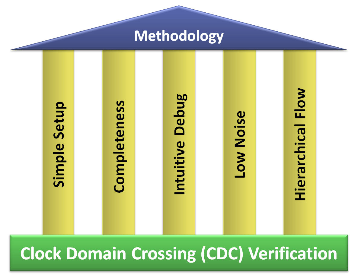
Figure 1: Ingredients of a Strong CDC Methodology
Here are the important ingredients of productive CDC verification for both ASICs and FPGAs:
In addition to these key ingredients, a proven methodology is an integral part of productive CDC verification. SoC designers may not be deploying all aspects of the methodology today but it is important to understand that these avenues are available to address the productivity needs of CDC verification.
There are various CDC verification solutions available in the market. One has to look at these important ingredients and a proven methodology to pick the most productive solution to enable design teams to manage the complexity and the time to market challenges for both ASICs and FPGAs.
 |
|
 |
 |
 |  |
 |  |
[…] Productive Clock Domain Crossing Verification What are the important ingredients of productive clock domain crossing verification for both ASICs and FPGAs? […]
[…] Productive Clock Domain Crossing Verification What are the important ingredients of productive clock domain crossing verification for both ASICs and FPGAs? […]