The latest architectural shift has significant implications for simulation and modeling of high-speed SerDes transceivers.

The ever-increasing demand for compute power and data processing in accelerators, intelligence processing units (IPUs), GPUs, as well as training and inference SoCs is driving the adoption of 112G SerDes PHY IP solutions. Ensuring a reliable Ethernet link and efficient integration are the most essential requirements that designers need to meet. IBIS-AMI modeling can help predict SerDes link performance and placement-aware 112G SerDes PHY IP can enable a more efficient SoC integration.
The IBIS-AMI modeling and simulation framework has enabled system and hardware engineers to verify off-chip interconnect designs by running simulations in an accurate yet efficient manner. Over time, the IBIS-AMI modeling process has been simplified with a variety of EDA vendors now providing add-ons to their existing simulator portfolio. An IBIS-AMI test bench offers a simple and fast way to ensure SerDes interoperability and link performance benchmarking.
Today’s PAM-4 112G PHY uses ADC-based flexible DSP architecture instead of a process, voltage, temperature (PVT)-dependent and hard-to-scale analog architecture. This architectural shift has significant implications on simulation and modeling of high-speed SerDes transceivers.
Figure 1 shows a typical 112G serial link implemented in a DSP-based receiver architecture. It consists of a transmitter (TX) with some finite-impulse response equalization (FIR) and a dispersive channel. The channel output is sent to a receiver composing an analog front-end (AFE), ADC, and a DSP block, which includes a feed-forward equalizer (FFE), a decision-feedback equalizer (DFE), clock and rate recovery (CDR), and an adaptation block (ADAPT). In such a design, a significant portion of the signal equalization comes after the ADC within the DSP.

Fig. 1: Typical ADC-based SerDes link.
Prior to ADC-based transceivers, the eye quality at the DFE slicer input was a good indicator of link performance. Therefore, an emulated continuous-time model of the waveform representing the DSP output is needed for the standard IBIS-AMI simulator to process and evaluate receiver performance.
The receiver IBIS-AMI model assesses the overall performance of the simulated link by returning an equalized analog signal as seen at the input of the sampler/symbol-detector. An IBIS-AMI model, with extended boundaries to include the ADC blocks and the equalization schemes implemented in the receiver DSP blocks, will encompass the full signal equalization chain to the final symbol detector where the performance metrics of the entire link are most relevant.
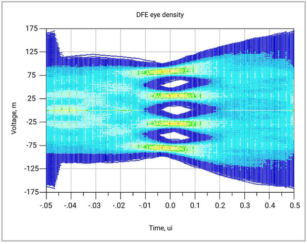
By incorporating a continuous-time emulated FFE and DFE in a model where the linear FFE is implemented with continuous delay blocks while the DSP coefficients are fed to the emulated FFE and DFE through DACs, existing IBIS-AMI models can emulate the DSP equalization and generate eye diagrams using inherent IBIS-AMI routines. An example of the subsequent emulated DSP EYE is shown in figure 2.

Fig. 2: IBIS-AMI analog waveform reconstruction.
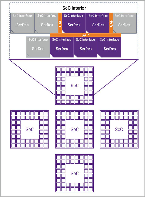
PHY macros serve as ports to an SoC to transmit data in and out, so the need for more bandwidth requires integration of a large number of macros. As such, all package signal escapes must occur via the beachfront, making it desirable to place the PHY macros on the beachfront to maximize data exchange rate per millimeter of die edge. The number of PHY macros in high-performance computing SoCs is approaching the limit to allow placement of all the macros on one edge of the die. In order to enable denser integration, it is essential to place multiple tiles of macros on all edges of the die. Figure 3 shows five SoCs with two tile deep stacking of SerDes PHYs.
Advance process nodes need unidirectional poly placement of all cells (transistors) that are placed in an SoC. Allowing both north/south and east/west orientation PHY placement needs careful consideration during PHY IP design, so the 112G high-speed SerDes PHY can be placed on all edges of an SoC.

Fig. 3: Two tile deep stacking of PHY Macro on all edges.
Compared to traditional NRZ, PAM-4 signaling is more sensitive to channel impairments such as noise, jitter, crosstalk, and non-linearity. Stringent 112G PHY interference tolerance/jitter tolerance (ITOL/JTOL) requirements present challenges related to signal routability. While keeping the number of package layers to a minimum to reduce packaging cost, the package designer must not only find ways to escape 100s of high-speed differential signals but also address issues related to power supply routing and supply bumps connections and formation of inductive loops when they are connected. The PHY IP bump map plays a crucial role in solving this issue. A placement-aware high-speed SerDes PHY IP that implements IP bump map to keep these constraints in mind during design phase enables denser SoC integration.
Synopsys provides silicon-proven PAM-4 DesignWare 56G/112G Ethernet and USR/XSR Die-to-Die PHY IP solutions that designers can integrate into their high-performance computing SoCs. Accurate IBIS-AMI models provide a way to evaluate link performance and channel margins with different channels.
Placement-aware, bottoms-up approach enables denser integration by allowing north/south and east/west placement with minimum number of package layers to reduce package cost. The high-speed SerDes PHYs’ flexible layout maximizes bandwidth per die-edge by allowing placement of macros in a multi-row structure and along all edges of the die.
Leave a Reply