Moving from 28nm to finFETs provides a 1.2X improvement in power and performance. Here’s how to get better results.

Recently Qualcomm announced their new SnapDragon processor 820, which was designed using finFET technology. They showed some amazing results, such as 2X improvement in performance and 2X improvement in power compared to 28nm designs. Previously, when ARM announced their A72 processors in finFET, they too had claimed 3.5X improvement in power compared to 28nm designs.
But can designers expect such dramatic improvement just by moving to finFET? Do they need to do anything more? If so, what extra steps do they need to do? We will be exploring these questions in this blog.
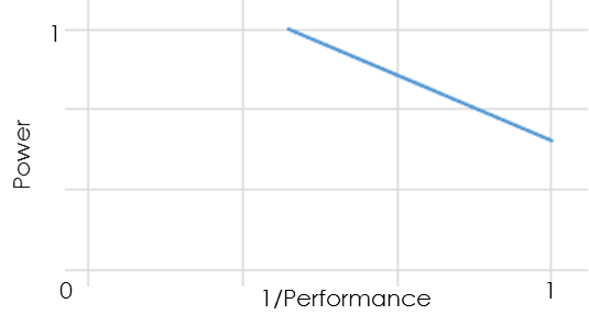
Let us look at the benefits of the finFET technology. FinFETs offer either a 1.38X improvement in performance using the same power or a 1.5X reduction in power at the same speed, when compared to 28nm process. If we were to draw a curve between these two points, it will appear something like what is shown in figure 1.

Figure 1: FinFET process benefits
From the above figure, we can find a point that gives the same scaling on both power and performance. This point denotes the benefits in power and performance just by migrating to finFET. Using this curve, we can find that it corresponds to 1.2X. This means, if we just migrate a design from 28nm to a finFET process, we should see an improvement of 1.2X on both power and performance.
How can we get even better performance and power improvement? Let’s discuss strategies to achieve power improvement for finFET designs.
In order to obtain power improvement, we should focus on the dominant component of power in finFET. Unlike 28nm designs, dynamic power dominates the total power consumption in finFET designs. When static power is dominant, as at 28nm, we want the smallest area possible. Conversely, with finFET, the larger the design area the less switching activity there is. Hence, the design choices we made in 28nm may not be effective and are often incorrect for finFET designs. Designers can achieve superior power improvement by keeping these principles in mind and following these strategies derived from them:
Using these strategies, both ARM and Qualcomm were able to improve upon power efficiency beyond what is offered “for free” by the finFET process. ARM used register file reorganization, power efficient tuning of execution units, and dynamic power reduction of every block to achieve greater power efficiency. Qualcomm used microarchitecture improvements like cluster multipliers and a number of dynamic power reduction techniques to achieve their numbers. What are your strategies for designing for power with finFETs? I would like to hear from you.
Leave a Reply