Significant progress is being made on a number of fronts.

Materials are fundamental to active photonics devices, and there were plenty of developments discussed at Photonics West 2014.
Element Six was happy to talk about progress in making large single-crystal diamond and even larger polycrystalline diamond wafers. Carbon has a number of stable forms; diamond, graphite, nanotubes and amorphous carbon. The Element Six process uses CVD conditions in which diamond and graphite are grown, but any graphite is immediately etched away so that only diamond is left. Done right, a very pure perfect single crystal is grown.
Diamond has two really useful properties (other than inducing loyalty): excellent transparency down to 220nm, and remarkable thermal conductivity. This enables windows for very-high-power CO² lasers used in Cymer’s EUV source, among other applications. These materials are now migrating to applications such as semiconductor laser and diodes, where the devices are very small and the local power density is high. A related example of application migration from high to low(er) tech was the introduction by Nikon of fluoride lenses, originally developed for 193 nm lithography, into smaller lower weight camera lenses .

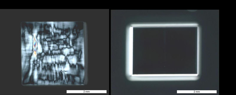
Improved low birefringence diamond, left = 10-4, right = 10-7 , from Element Six.
Aurelian David from Soraa talked about GaN grown on GaN, and homo-epitaxy rather than the standard hetero-epitaxy. The resulting improved crystal quality produced much better LEDs with spectacular 75% wall-plug efficiency. There were several more papers on GaN on large silicon wafers, which is the opposite strategy; large area wafers produce lower costs and live with poorer quality epi. Perhaps the most intriguing is work by Samsung and Seoul National University, where they separate the GaN layer from Silicon at the deposition temperature and avoid all of the stress from differential thermal expansion. They are making real progress on figuring out how to make decent LED, but “decent” is not “best”. It’s rather tacky, but in the cost vs. quality race, there is typically just one winner.
The solar cell is the other major photonics application in which materials are front and center. Silicon is firmly established as the incumbent solution. A team led by Yi Chen, from the University of Illinois at Urbana-Champaign, showed an improved moths-eye anti-reflecting top surface. They used a combined deposition and etch process to create resistant islands that acted as a mask to form pyramids on the cell surface. Perhaps this blog should have been on clever uses for simultaneous deposition and etch.
The best alternative to silicon is CIGS (copper indium gallium selenide), but obtaining consistent performance in volume has been the continuing challenge. A paper at the conference showed the uniformity of spectral output from CIGS cells using a “hyperspatial imaging” microscope. The spectral output was non uniform at the scale of µm’s, typical of crystal sizes. The paper was a good example of the power of the right analytical tool to provide insight.
Also on the solar materials front, but not talked about at Photonics West, “peroskovite” based solar cells have shown remarkable progress in three years. Peroskovite describes a crystal structure, and a particular stoichiometry has been found to have useful solar cell properties as a hole conductor. An absorbed photon creates an electron hole pair and the holes are preferentially conducted away. Because, they do not relay on a diode junction, a much wider range of wavelengths result in current. The remarkable story has been the improvement from 6% to 15% efficiency in three years. This sort of progress is always a very encouraging sign. The progress comes from materials discovery and improving the crystal quality based on growth on a TiO² layer. Because there is no junction diode, the 20% limit for a single junction diode does not apply to these materials so there is plenty of future opportunity. The issue appears to be materials cost, which manufacturing volumes usually fix, and lifetime.
All in all, an intriguing set of developments to keep the materials guys busy; try deposition and etch as the solution to any problem, make sure you can measure the results, and always improve crystal quality.
Leave a Reply