Creating a simplified thermal model that still accurately accounts for the details in each layer.

Driven by Moore’s Law and modern, ubiquitous computation power demand, the market will continue to demand higher chip performance. Therefore, modern chips with ever-higher power densities present critical thermal challenges. With the ever-shrinking design margins, designers must manage their thermal budget at every stage of the design, from chip to system.
Now, let us shift left and start at the chip level. Chip designs commonly use the Graphic Design System (GDS) file format. Since its inception, it has been the de-facto industry standard for data exchange of IC layout artwork. It is the final output of the IC design cycle. The GDS contains all the information of planar geometric shapes, text labels, and other information in the layout. The objects within a GDS file are grouped by assigning numerical attributes such as layer number or data type. This file contains everything that a foundry needs for IC fabrication.
However, since GDS files are binary, layer-based, and have an overwhelming amount of information, the challenges of using GDS design for thermal analysis are trifold:

Fig. 1: A rendering of a small GDSII standard cell with three metal layers (dielectric has been removed). The sand-colored structures are metal interconnect, with the vertical pillars being contacts, typically plugs of tungsten. The reddish structures are polysilicon gates, and the solid at the bottom is the crystalline silicon bulk. (Source)
In absence of optimal tools to accomplish all this, a common workaround is to treat the die as a block of silicon and completely ignore the metal layers and active devices on the die. It is actually not a bad approximation if you are trying to run system-level simulations. Another way to resolve a bit more detail is to model the die layers, with estimated material properties like thermal conductivity based on metal percentage of each layer. Again, not a bad idea when the scope is not at the chip or chip-package level. But what about the chip itself? These simplification methods won’t serve the purpose anymore.
Celsius Thermal Solver is a tool designed and developed by Cadence to help electrical and thermal engineers address their concerns. With Celsius, package, IC, and board designers and systems engineers will have the ability to transfer enormous amounts of information from within a GDS file into detailed, accurate inputs that are manageable for thermal analysis.
GDS files can be directly imported into a specially tailored version of XcitePI. No translator is required, only the Celsius Thermal Solver license. Here you can see the structures and details within each layer (see figure 2).
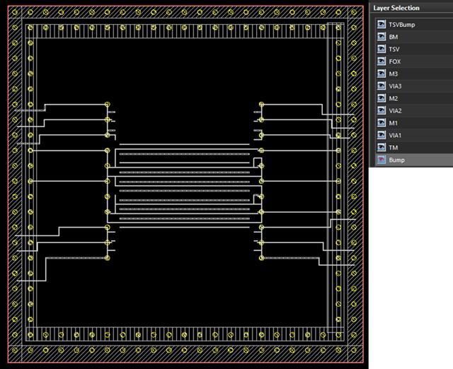
Fig. 2: An example of layer view of an interposer design in GDS format.
You can choose to keep all fine details, leading to incredibly large 3D thermal models that are normally computationally prohibitive. A much simpler but equally accurate way is to define a grid for certain layers, let’s say 20×25, and specify the metal and dielectric on that layer. The layer will be divided into 20×25 tiles, and within each tile an equivalent 3D thermal model will be calculated based on the details in that tile (metal shape, dimension, etc.). For certain layers, if there are large areas of metal whose shape and dimension are of special interest or critical for thermal performance, so that you want to keep the details, you can simply keep the metal shapes in that layer. The solder ball and bump layer is provided with an “extra refinement” option to capture those small cylindrical shaped structures. After specifying the level of resolution for each layer in the GDS file, you get yourself a simplified thermal model that most machines can handle and still accurately account for the details in each layer of the complex design for its thermal behavior.

Fig. 3: BEOL (metallization layer) and FEOL (devices). (Source)
The RAK (Rapid Adoption Kit), authored by Yanjun Xia, Sr Principal Application Engineer, is available at Cadence’s online support system and explains in detail how the information from GDS can be pre-processed and prepared for equivalent, effective, and efficient thermal analysis.
 |
|
 |
 |
 |  |
 |  |
Leave a Reply