A simple process that coats die and wire-bonded lead frames in an adhesion promoter helps ensure long-term reliability and performance.

Highly reliable power devices are always demanded by the automotive industry, especially with the surge in electric vehicle (EV) sales. These devices are expected to withstand harsh conditions and, at the same time, deliver consistent performances.
Interfacial delamination is a significant factor that can impact the reliability performance of power devices. It refers to the separation of layers at the interfaces of different materials within a device, which can lead to mechanical instability and degradation of electrical performances. This is particularly critical in power devices where multiple materials such as dies, die attach, wires, and lead frames are molded together. If delamination occurs, it can disrupt the electrical pathways, leading to device failure. Therefore, avoiding interfacial delamination is crucial for ensuring the long-term reliability and performance of power devices.
Efforts to mitigate the interfacial delamination issues are ongoing in the electronic packaging industry. The most common approach in counteracting the delamination issue is lead frame roughening technology [1, 2, 3, 4]. This approach roughens the surface of the lead frames mainly by micro-oxidation or micro-etching techniques. With the roughened lead frame surfaces, the epoxy mold compounds (EMCs) can grip better on the lead frame resulting in better adhesion through the mechanical interlocking mechanism. While these roughened lead frames are effective, the technology often involves the use of hazardous chemicals and sizeable equipment footprints with complicated processes including pre-cleaning, roughening, and post-cleaning of the lead frames. It is also found that the die attach epoxy tends to bleed out on roughened lead frames which, in turn, means a negative impact to the device’s reliability. Hence, a die attach or lead frame treatment with anti-bleed property is needed [3, 4].
In this study, the authors propose another simpler and more economical approach than the lead frame roughening technology to achieve zero interfacial delamination equivalent to the lead frame roughening technology. Additionally, this technique does not have the die attach epoxy bleed out issues like the roughening technology. Fundamentally, this approach coats a layer of adhesion promoter (AP) on the die and wire bonded lead frames to enhance the interfacial adhesions. Since the adhesion promoter is coated after the die and wire bonding processes, all materials interfaces including the die, wire, solder, and lead frame with the epoxy mold compound are covered. Unlike the lead frame roughening technology, which just focuses on the lead frame, this total molding surface adhesion promoter coating’s inclusiveness can eliminate the seed of delamination from growing on all possible interfaces.
Generally, the adhesion promoters must be able to bond inorganic materials like the dies, wires, solders, and lead frames to the organic epoxy mold compounds. To this end, silane (silicon-hydride) coupling agents are suitable candidates for the adhesion promoters as they are widely known to be the adhesives to chemically bond the inorganic and organic materials [5, 6, 7, 8]. The silane coupling agents are molecules containing silicon-hydride (SiH) groups and another organic chemical functional group. To attach, the SiH groups form covalent bonds with the hydroxylated oxide layers on the inorganic materials under the presence of water, while the chemical functional groups cross link with the functional groups in the organic materials. Due to this unique chemical structure, it enables covalent bonding with both inorganic and organic materials. Silane coupling agents fit as adhesion promoters to be coated on the power devices, which consist of a combination of inorganic and organic materials.
Evaluations conducted on the adhesion promoter coated power devices in this study show that the devices are free from interfacial delamination even after the stringent moisture sensitivity level (MSL) 1 conditioning. It is also worthy to note that the coating method just requires dipping the die and wire bonded lead frames into the bath of adhesion promoter – a very simple process. In essence, the adhesion promoter coating proposed by the authors is effective and easily implemented for high power devices. The details on the coating and the reliability performance of the coated devices are presented in later sections for better understanding.
The D2PAK package is selected as the test vehicle in this study with the dimension of 14 × 19 × 4 mm3. In this package, 6 × 4 × 0.2 mm3 silicon carbide (SiC) dies are bonded on the 12 × 9-mm2 die pads. Adhesion promoters are coated on the devices after wire bonding to strengthen the epoxy mold compound’s adhesion to the devices.
Figure 1 shows the devices fabrication process flow.

Fig. 1: SiC D2PAK devices assembly process flow.
With the intent to avoid interfacial delaminations due to the stresses during the device’s fabrication and operating conditions, the AP is coated on the devices after the wire bonding process to enhance the interfacial adhesion strengths.
This process coats a layer of a self-assembly monolayer (SAM) on the surfaces of the devices as adhesion promoters to chemically bond the organic EMC to the inorganic copper (Cu) lead frame, SiC dies, aluminum (Al) wires and high lead (Pb0 solders. Figure 2 illustrates the typical structure of the SAM. It consists of three main parts which are the headgroup, backbone, and endgroup. Brief descriptions on each of the parts are presented as follows [7].
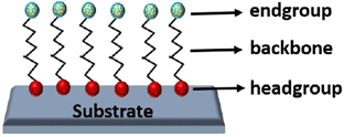
Fig. 2: The typical SAM structure [7].
In this study, to improve the adhesion strengths of the different interfaces in the device, (3-Aminopropyl) triethoxysilane (APTES), a species of amino silane coupling agents was selected for the AP. The amino endgroups in APTES can form covalent bonds with the epoxy and phenol chemical groups, respectively, in the common epoxy mold compounds [9]. These covalent bonds serve as the chemical linkages between the EMC and other inorganic materials in the devices, which are bonded through the salinization reaction using the APTES headgroups [7, 10].
The APTES AP coating occurs by dipping the die and wire bonded lead frames into a bath of APTES diluted by a mixture of isopropyl alcohol (IPA) and deionized (DI) water, as shown in figure 3. It is vital to note that a suitable solvent ratio of IPA:DI water and concentration of APTES are important factors to avoid the unwanted polymerizations of the APTES on the surfaces, weakening the adhesive properties [6, 8].

Fig. 3: Dip coating of die and wire bonded lead frames.
Since this coating is a self-assembled monolayer (SAM0, the thickness is too thin to be measured or detected directly using optical microscopes. Hence, in this study, X-ray photoelectron spectroscopy (XPS) is employed to detect the presence of the APTES SAM, similar to the previous studies in the literature [10].
Table 1: Elemental Analysis of APTES Coated Lead Frame
| Sample | Atomic Composition (%) | ||||
| Cu | C | O | N | Si | |
| Cu Lead Frame | 10 | 52 | 34 | 4 | 0 |
| APTES Coated Cu Lead Frame | 2 | 59 | 26 | 7 | 6 |
Through the elemental analysis by XPS, the atomic composition on the lead frame surfaces can be identified and are tabulated in Table 1. It is observed that the Si is detected on the APTES coated lead frame, while it is not detected on the non-coated lead frame. Owing to the presence of the Si element in the APTES chemical structure (shown in figure 3), it is a clear indication that the APTES is coated on the lead frame.

Fig. 4: Chemical structure of APTES.
Aside from the sophisticated XPS, solvent contact angles and surface energies are also measured for the coated and non-coated lead frames in this study. It is found that the APTES coated lead frames have lower contact angles and higher surface free energy than the non-coated lead frames as indicated in Table 2.
Table 2: Contact Angles and Surface Free Energy
| Sample | None Coated Cu Lead Frames | APTES Coated Cu Lead Frames | ||
| Solvent | DI Water | Solvent A | DI Water | Solvent A |
| Contact Angle (o) | 90 | 57 | 63 | 38 |
| Representative Image | ||||
| Surface Free Energy (mN/m) | 33 | 51 | ||
The lower water contact angles of the coated lead frames are associated with the nature of the APTES SAM as elaborated below [11].
In addition to the elemental analysis and wettability study on the APTES SAM, visual inspections on the coated lead frames after baking were conducted as well. Figure 5 shows the appearances of the lead frames after baking. It is found that the non-coated lead frames are oxidized, as evidenced by the grey-purplish appearance. Nevertheless, this grey-purplish appearance is not observed on the coated lead frames. Instead, the lead frame surfaces appear to be brown in a brighter tone. This observation is likely due to the curing effect of the APTES SAM to the lead-frame surfaces.

Fig. 5: Appearances of baked (a) non-coated and (b) coated Cu lead frame.
Since the AP coating is conducted through dipping, the entire lead frame is fully coated including the leads and exposed pads which are to be tin (Sn) plated. The effects of the APTES SAM on the plating quality are evaluated through checking the Sn thickness and solderability of the singulated units.
Table 3 shows the output responses of the inspection items on the singulated units after Sn plating. The AP coated units meet all the quality requirements after Sn plating—identical to the non-coated units. This suggests that the cleaning processes before Sn plating are sufficient to remove the APTES coating.
Table 3: Inspection Items for Sn Plating Process
| Sample | Sn Thickness | Solderability | |
| After 8 Hours of Steam Aging | After 4 Hours of Dry Baking | ||
| Non-Coated Units | Within Specifications for Leads and Exposed Pads | Fully Solderable on Leads and Exposed Pads | |
| AP Coated Units | |||
The AP coated devices are subjected to both IPC / JEDEC moisture sensitivity level (MSL) 1 and 3, respectively, with the addition of 1,000 thermal cycles (TC) reliability conditioning. After the conditioning, scanning acoustic tomography (SAT), non-destructive testing, is employed to probe the internal structures of the units for interfacial delamination inspections. Table 4 tabulates the quantity of delaminated units after reliability conditioning for the non-coated and AP coated units, respectively. The non-coated units have a significant number of interfacial delaminations, while all the AP coated units are free from delamination after reliability stresses.
Table 4: Quantity of Delaminated Units
| Sample | Reliability Condition | ||||
| T0 | MSL 3 | MSL 3 + 1,000 TC |
MSL 1 | MSL 1 + 1,000 TC |
|
| Non-Coated Units | 14 / 36 | 12 / 15 | 15 / 15 | 15 / 21 | 21 / 21 |
| AP Coated Units | 0 / 36 | 0 / 15 | 0 / 15 | 0 / 21 | 0 / 21 |
To further understand on the interfacial delamination of the units, the SAT images of the units are reviewed and presented in figure 6. The delaminated interfaces are highlighted in red color. Note that the interfacial delamination of the non-coated units started on the peripheral of the die paddles since T0. After MSL 3 conditioning, the severity of the die paddles peripheral delamination amplifies without extending to other regions. On the other hand, after MSL 1 conditioning, the units are observed to have delamination at edges of the dies on the die paddles aside from the delamination at the die paddles’ peripheral. This delamination at die edges on die paddles is only observed for units conditioned under MSL 3 after 1,000 thermal cycles. The higher severity of the delamination under MSL 1 conditioning is expected due to the more stringent conditioning.

Fig. 6: Progression of the interfacial delamination after reliability stresses.
There are many factors that could lead to the interfacial delamination of the devices. Some of the major factors are briefly elaborated as follows [12].
Through the AP coating on the devices in this study, it is found that the interfacial adhesion is strengthened resulting in the zero interfacial delamination even after the MSL 1 conditioning.
This study proposes a straightforward and effective method to improve the adhesion strengths of material interfaces in power devices through the application of an AP. The AP is a layer of APTES SAM coated on the die and wire bonded lead frames to enhance the adhesion strengths of the material interfaces.
This APTES SAM can be coated on the lead frames by dipping them in a bath of diluted APTES. The results indicate that this AP coating is effective in bonding various materials in power devices, including SiC dies, high Pb solders, Al wires, and Cu lead frames with the EMC. It is observed that devices coated with AP show no signs of interfacial delamination even after undergoing rigorous MSL 1 reliability stress conditioning. This suggests that the AP coating method is a promising solution for enhancing the reliability and performance of power devices.
 |
 |
 |
|
 |
 |
 |  |
Leave a Reply