For AI compute, simply throwing more chips or processors at the problem is not a scalable solution.

Data centers, autonomous vehicles, and computer vision applications are pushing the limits of scalable AI compute. Data center chips face multi-trillion parameter models that continue growing every year. ADAS systems require flexibility and processing power for new model types, such as vision transformers. Edge AI solutions demand tight power budgets and the ability to process multiple models in parallel. System architects are finding that the old way of throwing more chips/processors at the problem does not lead to a scalable solution.
Why is conquering AI hardware so tricky? AI models are advancing in size and complexity at a hockey stick growth rate, and hardware compute capabilities are not keeping pace. Let’s look at Nvidia’s product roadmap as an example. Recently, the AI behemoth announced its Hopper GPU lineup. Compared to its previous Ampere GPUs, the company claims that its new hardware improves training times by more than 2x and inferencing rates by ~2.5x. While these growth rates are very impressive, they pale in comparison to model size growth.
The tried-and-true means to increase performance has been to multiply the number of tiles, cores, or chips. AI chips follow this time-tested method, and hardware solutions—especially in the data center—can exceed 850,000 cores per chip (Cerebras’ WSE2). But the problem is as designers add more processing elements and chips to tackle these models, the performance per core declines, as figure 1 highlights.
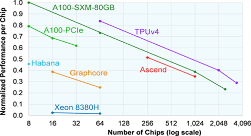
Fig. 1: Performance per chip. (Image source: TechInsights)
These diminishing returns are due to the inherent overhead in multiprocessor implementations. System designers have explored many angles to improve scaling, such as different memory technologies, high-efficiency interconnects, and software optimizations. However, one crucial design aspect often gets overlooked: the clock network. The seemingly mundane technology can account for 30-40% of power consumption and it has an impact on data movement architectures, frequency scaling, and design complexity.
In the era of AI, large multicore chips are the new normal. More tiles or cores require more area, leading to many downstream problems, such as higher power consumption, more complex interconnects, higher system latency, and increasing skew. These problems stem from inefficiencies in existing clock network solutions.
Imagine that you were hit with a transformation ray and became a clock signal in a 500mm2 chip. As you begin your long and winding journey to a MAC unit, you will encounter repeater flops across the NoC, synchronizing flops between the AI engine and NoC, and CDC cells as you traverse clock domains. Each of these stops creates at least a single cycle of latency, and large chips have hundreds of thousands of these points, if not millions. All of these add to clock network overhead and notable increases in system latency.
Architects and physical design teams often work independently, leading to a disconnect when addressing design constraints. While some of the previously mentioned issues reside in the timing domain, they can derail progress towards stretch performance and architectural goals. For example, an architect may push for a fully synchronous chip. But, if there are limitations of the clock distribution network, physical design teams might not be able to implement a fully synchronous domain across a large chip and meet frequency goals. The back-end engineers would have to revert to asynchronous domains, introducing unwanted latency and stymieing performance growth.
This divide-and-conquer methodology squeezes physical design teams to realize performance goals set by the architect. But if we approach the problem holistically, there is an opportunity for the entire design team to meet stretch performance goals without kicking the proverbial can to the back-end design team.
Every chip starts with a perfect clock signal. As the signal travels through the chip, it is often delayed and distorted because of the chip’s electrical properties. But what if there were a way to actively compensate for these problems caused by the inherent physics of the chip so that we could deliver a perfect clock signal closer to every flop? This technique is the approach Movellus takes with its intelligent clock network IP. Intelligent clock networks strategically place smart clock IP modules throughout the chip. These modules actively compensate for on-chip variation, skew, and aging during runtime. Smart clock modules are also aware of other smart clock modules and can synchronize to create large synchronous clock domains. This approach reduces the need for retiming flops, CDC buffers, and repeater flops, thereby avoiding overhead and affording lower latencies for AI applications.
Figure 2 compares Movellus’ intelligent clock network approach with today’s popular solutions, including a tool-driven methodology with clock tree synthesis (CTS) and a semi-custom strategy that implements a mesh. The chart shows design tradeoffs regarding Fmax, useful clock period, process flexibility, power and area efficiency, and ease of timing closure. Intelligent clock networks can bring the combined advantages of today’s solutions by offering the performance of a mesh at the power consumption of a tree.

Fig. 2: Clock network design approaches.
Taking a holistic approach to clock network design and using a solution such as Movellus’ intelligent clock network solution can significantly enhance performance, power efficiency, and area efficiency compared to existing solutions. A key architectural advantage is that intelligent clock networks enable the expansion of synchronous clock domains. These networks allow SoC designers to remove unwanted and accumulating system-level latency for larger chips by eliminating overdesign for your clock network. As architects strive to meet the compute requirements for larger and more complex models, they must reexamine each barrier against efficient scaling, including the clock network. Intelligent clock networks provide an architectural solution that enables chip makers and OEMs to scale their AI compute designs to meet the needs of future generations of products.
 |
|
 |
 |
 |
 |
Leave a Reply