Lots to talk about from SPIE Advance Lithography Conference this year; EUV power, multi-beam systems, double patterning, and imprint. I thought I would pick up some highlights here, and then come back and talk about them in detail over the next few weeks.

by Michael P.C. Watts
Lots to talk about from SPIE Advance Lithography Conference this year; EUV power, multi-beam systems, double patterning, and imprint. I thought I would pick up some highlights here, and then come back and talk about them in detail over the next few weeks.
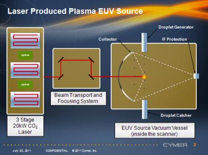
One of the extreme sources was the paper from Cymer/ASML on EUV sources . Their paper showed performance, at production duty cycles and control, that represented something like 30 x 300mm wafers an hour for 8 hours. This is a real breakthrough from just 4months ago ; a 2x increase in power, a 5x improvement in control, and 2x in duty cycle. They still need another 5x in power, and claim a retrofit upgrade path. The eye popping number (based on a little back calculation) is the wall plug peak power of the final box at 0.5 Mega-watt (that is not a typo).
The other extreme sources are all the multiple beam e-beam machines. I sat in on the KLA talk about their REBEL system. This is the system with 10’s of wafers, under 10’s of heads, each head with 10’s of thousands of beams. The 10’s of thousands beams are switched on a wafer scale electron mirror device.
This year’s progress is that they have now obtained functioning large mirrors and are showing patterned resist lines. The lines are rather large at around 100 nm feature size. Real progress, but a huge mountain to climb as they just have to…….. get to performance on a single head, integrate heads, confirm alignment, throughput, defects, oh and demonstrate reliability.
All sorts of papers about block copolymers and directed self-assembly (DSA). This is both potentially a lower cost path to double pattern, but also a very low cost subject to do research on ! The device guys showed that they can control the directed part to create real device like patterns. Kurt Ronse from Imec told me that all of his defect work suggest that there is nothing unique about DSA defects, and defect density targets will be met. I thought the most interesting paper was from IBM/ARM, when the ARM guy talked about the design impact of design rules that come along with double patterning. He expects that 4 more metal layers will be needed to work around the design rule limitations at 10 nm node (that’s 60 atom wide) features. The consequences of future rules had him “too busy weeping in beer to care !“.
Several papers and supplier talked about resist cleaning and filtering, a subject that does not often get talked about in these academic circles. The team from Molecular Imprints (MII) are installing resist cycling pump systems as part the next set of defect reduction fixes. The continuous c ycling polishes resist in a reservoir. Elsewhere at the conference, Entegris published a series of defect reduction studies on resist cycling systems, and ATMI announced a new plastic bottle with low particulates and trace metals.
MII identified resist particles as one of the next fixes in continued improvements in defect density that have now yielded single strands of metal interconnect 10m long. If progress continues at the current rate, they will hit production defect numbers in 2 years. In addition, MII partners are delivering a 6 headed cluster tool next year. It is clear that at least 1 flash memory end user is committing significant money to imprint.
I walked away from the conference with complete confidence that 10 and 7 nm node will be patterned one way or another, probably using 193 nm light and DSA double patterning. However, the cost of patterning and the design rule impact is so severe that the $ per transistor may not improve, stalling the cost driver of Moore’s law. A successful alternative to double patterning will have a huge impact. EUV power took a big step forward that will encourage the logic guys. Imprint has a real chance in memory, but multi-beam e-beam has a much longer path to success for foundries.
About the Author—Mike Watts has been patterning since 1 um was the critical barrier, in other words for a longtime. I am a tall limey who is failing to develop a Texas accent here in Austin. I have a consulting shingle at www.impattern.com.
My blog “ImPattering” will focus on the latest developments in the business and technology of patterning. I am particularly interested in trying to identify how the latest commercial applications evolve.
 |
|
 |
|
 |
 |
 | |
 |
 |
Leave a Reply