Achieving high package integration with routable leads and high heat dissipation.

For high performance applications, demand for highly integrated packages has increased. This is due to the highly integrated package’s electrical performance advantages of reduction of interchip distance (delay), high density I/O counts for multi-function and small form factor [1-3]. With the increasing importance of highly integrated packages, the need for improved thermal management is also increasing. When the high-density I/O signals operate for the highest performance, heat generation increases on the die. The high heat generation without effective heat dissipation has adverse effects on reliability and electrical performance of electronic products [4].
The MicroLeadFrame (MLF)/quad flat no lead (QFN) package, which is a Chip Scale Package (CSP) fabricated from one-layer leadframe, has been used in various applications for many years [5]. The MLF or QFN is famous for high reliability and high heat dissipation from a thick copper (Cu) alloy exposed pad which has high thermal conductivity at the bottom of package. This design supports reduced die temperatures [6]. However, it is hard to apply the QFN in highly integrated package with high density multi-functional I/O counts due to the peripheral leads of QFN. The QFN leadframe cannot have formed routing leads because of its etching process [7-9].
To overcome the limitations of QFN design, a routable (thin) MicroLeadFrame (rtMLF) package with routable connections is introduced. The process flows of QFN and rtMLF substrates are shown in figure 1. Comparing the two substrates, the conventional substrate has top and bottom etching before surface finish (figure 1(a)) while the rtMLF substrate has etching performed first at the bottom only followed by pre-resin filling and grinding. After top etching, the top pattern remains, including the routable internal leads without exposing the bottom (figure 1(b)) [7]. The conventional leadframe substrate may also be configured with internal leads, but their length is limited because they have no stable support at the bottom. In contrast, an rtMLF substrate can be configured with internal routing leads because the pre-resin supports the bottom of the internal routing leads. Therefore, it is possible to increase design flexibility of rtMLF packaging and it can be applied to various applications. Recently, the rtMLF technology has been researched as a wettable flank package with pre-resin supporting and electromagnetic interference (EMI) shielding package using isolated pads for automotive applications [8, 9]. However, a highly integrated package for multi-functional I/O counts with multi dice has not been studied with rtMLF technology and its internal routing leads.

Fig. 1: Steps in the fabrication of package substrates.
In this study, a new package structure which is a multi-chip module (MCM) rtMLF was researched. The MCM rtMLF design layout was proposed according to multi die interconnections with internal routing leads between two dice with two individual exposed pads. Testing provided verified enhancement of its small form factor compared with two single QFN packages. The designed MCM rtMLF samples were tested for their feasibility. Then, various reliability tests for automotive use were performed to verify the structural rigidity. In addition, electrical simulations were performed comparing two single QFN packages mounted on a board with MCM rtMLF. Furthermore, thermal simulation about thermal resistance of MCM rtMLF was conducted to compare it with MCM two-layer chip scale packages.
Information for the test vehicle is summarized in table 1. Most descriptions are similar to a conventional QFN. Using this test vehicle, layout on board was compared with two single QFN packages. The layout of two single QFN packages consisted of 7 X 7 mm2, 9 X 9 mm2 body using 8.5 mm2 and 9.1 mm2 dice size, as shown in figure 2.
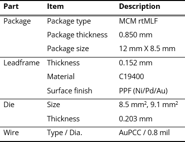
Table 1: Test vehicle dimensions and description.
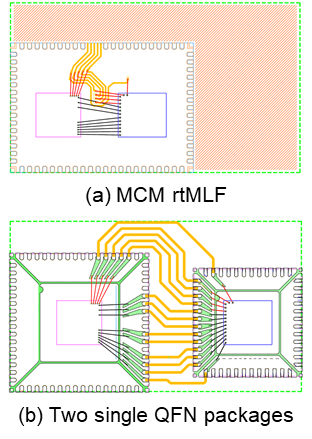
Fig. 2: Package layout on the printed circuit (PC) board.
In the former case, the two dice are connected by internal routing leads in the package, so there is no need for additional connections on the board (figure 2(a)). Whereas, in the latter case, Cu traces must be designed on the board for the connections of two dice with 3-mm distance (figure 2(b)). The area of two single QFN packages including board connections is 211.38 mm2 and that of MCM rtMLF package is 102 mm2. Thus, at least 51.75% board space can be saved by using the MCM rtMLF package. From this analysis, enhancement of small form factor through MCM rtMLF packaging was confirmed.
Process flow of MCM rtMLF from table 1 is shown in figure 3. The left side presents fabrication of a substrate with routable leads. Initially, the Cu alloy leadframe was the same as the QFN substrate. Secondly, the rtMLF substrate was bottom etched leaving exposed pads and leads. During bottom etching, the region of long routable internal leads was also etched, and it remained after the top etching process. Thirdly, pre-resin filling on the bottom etched area was performed to support the remaining top region. Grinding the overfilled pre-resin exposed the package leads. Finally, routing of the internal leads was performed after top etching. As a result, the internal routing leads could be left during fabrication since they were supported by the pre-resin. The right side of figure 3 shows assembly process of the MCM rtMLF package, which is the same as the QFN process. Two dice were attached on separated individual exposed pad and cured at the same time. After this, wire bonding and molding processes were conducted to confirm feasibility of MCM rtMLF design.

Fig. 3: Process flow of MCM rtMLF.
In the assembly process, wire bonding was key to confirm the feasibility of the MCM rtMLF design. Internal routing leads for die-to-die interconnections were positioned far from package pin area and floated from the bottom side. Thus, wire bondability was needed essentially for confirming the feasibility of structure and package reliability. After wire bond optimization, the measured stitch pull of the internal routing leads was over 6 g, which is above the minimum requirement. The wire bondability and moldability are shown in figure 4. From these results, the feasibility of MCM rtMLF design was confirmed.

(a) After wire bonding (b) After molding

(c) Cross-sectional image after MCM rtMLF process
Fig. 4: Feasibility of MCM rtMLF packaging.
After assembly process, package level reliability tests were conducted on the MCM rtMLF package. The reliability testing is based on the Automotive Electronics Council Q006 (AEC-Q006), which is for Gold Flash Palladium Coated Copper (AuPCC) wire packages. Moisture sensitivity level 3, thermal cycle H, unbiased highly accelerated stress test and high temperature storage test were conducted for MCM rtMLF. During the test, structure failure such as delamination was checked by scanning acoustic tomography inspection in each reading point. And results of inspection show all passed. The reliability items, conditions, reading points, quantity and result are summarized in table 2.

Table 2: Result of reliability (AEC-Q006) tests.
Electrical simulation test vehicles were designed the same as in figure 2. The Ansys Q3D 2022R1 simulation tool was used for the electrical simulation tool to compare resistance, inductance and capacitance (RLC) parasitics between the two test vehicles under 1 GHz frequency conditions. The measured nets were composed of die-lead-die connections in package or die-Cu trace-die on the board (net #1, #2), and die-die connections in packages or die-Cu trace-die on the board (net #3, #4) as shown in figure 5. Also, scattering parameter (S-parameter) of net #1, #2 were measured by Ansys HFSS 2022 R1 simulation tool from 10 MHz ~ 1 GHz frequency.

Fig. 5: Test vehicles for electrical simulation.
The RLC parasitic values for MCM rtMLF and those of two single QFN packages were summarized in table 3. The measured values of MCM rtMLF drastically decreased compared with two single QFN packages with about 35% of resistivity and 40~50% of inductance. Furthermore, the decrease of capacitance was about 35% and 54% in each die-lead-die connection (net #1, #2) and 85% in die-die interconnections (net #3, #4). These RLC reductions occurred due to shorter interconnection lengths. Insertion loss comparison of test vehicles is shown in figure 6. At the 1 GHz, insertion losses of MCM rtMLF, which is shown by two solid lines, are lower than those of two single QFN packages, which are shown by dotted lines. In conclusion, the electrical performance of MCM rtMLF is better than two single QFN packages.

Table 3: RLC parasitic after electrical simulation

Fig. 6: Insertion loss of test vehicles.
Usually, most of the heat generated from the die is dissipated through the board [10]. This thermal simulation was done to evaluate and compare capabilities of thermal performance for MCM rtMLF and MCM two-layer CSP structures in each different power levels. Figure 7 shows schematics of thermal simulation test vehicles. The schematics of the simulation structures were shown in figure 7(a)~(d). In this simulation, the package outline of thermal simulation structure was the same except for the die pad structure. For the MCM rtMLF, exposed pads for heat dissipation were composed of thick Cu alloy (figure 7(b)). However, those of the MCM two-layer CSP packages were composed of thermal vias (w/o via fill, w/ via fill) as shown in figure 7(c, d). The thermal simulation followed JEDEC (JESD 51-2A) set up for still air environment (figure 7(e)).
Table 4 summarized the result of thermal simulation comparison between MCM rtMLF and MCM two-layer CSP structures. Theta JA, the thermal resistance, is a parameter for showing heat dissipation performance. Based on the thermal simulation result, theta JA of MCM two-layer CSP packages is about 20% higher than that of MCM rtMLF for each die power. Figure 8 shows the temperature distribution on package surface when power per die is 1 W. The temperature of dice of MCM two-layer CSP packages is about 10% higher than that of MCM rtMLF. Consequently, the MCM rtMLF package shows higher heat dissipation performance than that of MCM two-layer CSP packages.

Fig. 7: Thermal simulation setup.

Table 4: Result of thermal simulation.

Fig. 8: Temperature distribution of package surface (1 W).
High package integration is one of the driving forces for high performance and small form factor packages. With increasing of multi-functional I/O density, the importance of thermal management is also increasing. In this study, MCM rtMLF is suggested for high integration with internal routing leads to connect die to die and high heat dissipation. Internal routing leads are supported by a pre-resin which is filled during substrate fabrication. It can overcome the limitations of a conventional QFN design.
From this research, the feasibility of the MCM rtMLF with internal routing leads was checked. The actual MCM rtMLF passed AEC-Q006 reliability test. Through electrical simulation comparison between MCM rtMLF and two single QFN packages, higher electrical performance of MCM rtMLF was verified. In addition, high heat dissipation property of the MCM rtMLF was checked by comparing with MCM two-layer CSP designs.
The routable molded leadframe can provide a highly integration solution with high heat dissipation. The application of integrated rtMLF will be expanded in various markets.
 |
|
 |
|
 |
 |
 | |
 |
 |
Leave a Reply