The path to making engineers more productive and speeding time to high-volume manufacturing.

Global internet traffic is growing exponentially, with no sign of slowing, and this demand is driving the evolution of the semiconductor industry. The appetite for more and more data requires sensors for capturing the data, networks for moving the data, storage, and processing power to analyze the data. As the demand for data grows, the underlying technologies must advance to not only meet today’s needs but address the applications of the future.

New Technologies Are Driving Innovation in Complex Digital Devices

The historical growth of transistors per microprocessor demonstrates that the pace of processing demand as expressed by device complexity has also continued on an exponential growth path for fifty years. New applications demanding more processing power are key drivers of this trend, and the future, with applications like augmented reality, will continue to make demands on performance. With more devices on advanced nodes and more demand for these chips, investments in advanced semiconductor fabs have nearly doubled in the past year to a new level of more than $100B USD. The increase in production drives demand for quality automated test equipment (ATE) and the increase in chip complexity is driving new challenges for test.

Looking back at semiconductor test over time, the challenge in the 1990s was just being able to functionally test the device. The next era was focused on cost reduction utilizing higher throughput test equipment with lower test times and higher parallelism. And the last few years have been characterized by increasingly complex semiconductor fabrication processes and packaging trends (starting with Intel’s move to FinFETs in 2011 for 22nm). We expect this to be the primary driver impacting test through the end of this decade at a minimum.
One of the latest breakthroughs in semiconductor device fabrication sees the evolution from 2D structures into ever more intricate 3D structures, like Gate-All-Around (GAA) FET transistors. Since test is really about finding manufacturing defects, these new and very fine device structures require more types of subtle defects to be found, increasing test complexity. The transistors continue to become smaller and with many more of them on a die, we are seeing increasing switching currents. We’ll come back to that though.
First let’s talk about the fact that more transistors dictate greater memory depth, leading to new digital test techniques, which require new digital instrumentation. This, however, will be quickly addressed by all major vendors so let’s look to another level of challenge that will need to be addressed.

Returning to the increasing switching currents discussion, a less obvious impact with the adoption of advanced process nodes is the impact on tester power supplies for the device. The act of turning a transistor on and off looks like charging a really small capacitor – a small charging current. But when you add up 10, 20, 50 billion transistors that’s a lot of instantaneous current. We’ve seen devices that pull up to 2000 Amps of instantaneous current, and yet as the process node advances the operating voltage declines. This declining voltage while simultaneously switching huge currents is one of the biggest challenges in testing advanced digital devices, which brings us to a controversial conclusion – that the toughest challenges in digital test are really analog problems.
Building up a high bandwidth interface with a conventional power supply requires building an elaborate network of carefully matched capacitors, paying attention to resonant frequencies. The alternative and only real solution for test engineers is a dynamic power supply to reduce the effort and make the application’s hardware work the first time. Digital test is really about having the best analog solution.
3D Device Structures Driving the Need for System Level Test

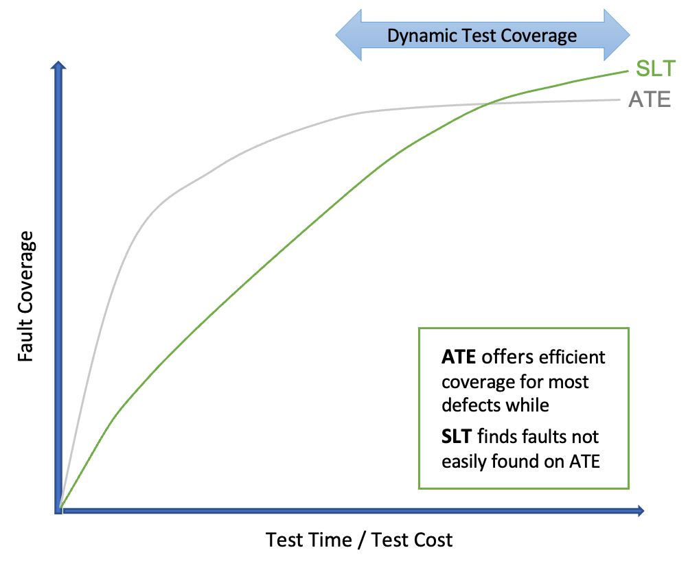
Let’s now turn our attention to that fact that these intricate 3D device structures create multiple new defect modes and these defect modes are very challenging to find with conventional test methods. Defects may only show up in mission-mode testing, and this is where System Level Test (SLT) equipment has a growing importance for advanced digital devices.
System Level Test is not a replacement for conventional ATE, nor is it an additional test insertion. Fault coverage on ATE is fast and efficient, up to a point, after which it takes significantly longer to find more subtle defects. SLT, on the other hand, has a more linear fault coverage over time initially but some of the more subtle defects can be found in less time than ATE. The future will see an optimization of test coverage between ATE and SLT. Our recent System Level Test 3 for 3 video short examines use cases and emerging trends for System Level Test.
In addition to the discussion of these technical hurdles in testing advanced digital devices, we should also ask ourselves whether this is really the biggest challenge facing the semiconductor industry. We’ve all read that the industry faces the reality of the limits of rare earth resources, like lithium and cesium, but historically, replacement technologies have been developed to offset material shortages. But let’s consider another rare resource in our industry – the engineer. With a shortage of quality engineers and the industry growing exponentially, it is imperative that we consider strategies for minimizing the impacts of human capital on the industry’s growth potential.
We could look at the approach that is taken today with rare earth minerals – increase production through mining. We could ask our educational institutions to increase production – and they are doing that – but it takes time. More time than we probably have.
Artificial intelligence is another trending topic. It has come a long way in a relatively short period of time and while it may one day be assisting engineers in code generation by automating some of the more standard and repetitive tasks, it’s unlikely AI will fully replace the engineer in the near future.
But we can make our existing engineers more efficient, increasing their productivity. Today’s test engineers are faced with constant pressure to reduce the time it takes to ramp from design to high volume manufacturing, and then maximizing throughput and yield. Complexity is inherent throughout this process and so choosing solutions that minimize this complexity can result in significant gains in productivity. Teradyne products are engineered with this in mind and include innovative solutions that speed time to market and maximize yield.

A good place to start is by reducing the complexity of the test engineer’s job. What if there was a well-designed tester that allows each site to have the same symmetrical design, eliminating the need for a multi-site interface board, and ultimately reducing DIB design complexity? This means less design effort, much better correlation from site to site, and a basic simplification of the design that allows the test engineer to focus on the test list and the device being tested.
Teradyne’s Broadside applications interface on the UltraFLExplus delivers just this, ensuring the large PCB area for DIB circuitry is placed between the instrument connections and the DUT (as compared to pushed off to the sides of the PCB), which truly enables site to site copy/paste placement, and resulting layout consistency. This simplicity saves test engineers DIB design time but even more importantly, avoids the risk of longer debug times for multisite issues – or worse yet, having to re-spin a DIB due to a site to site design issue. With faster time to correlation while matching multi-site performance, the Broadside interface reduces engineering effort to produce a production-ready test program by >20% and increases manufacturing productivity with 15%-50% fewer test cells. By simply simplifying the architecture, engineers become more productive.
Data is another area that can be leveraged to improve factory productivity. In some cases, you need low latency, fast decision-making that is in-line with the test flow, requiring a local solution that is tightly integrated with the tester. Other data factoring needs to go to the cloud or to the factory MES system. This data wants to operate on the customer’s software systems so that the actions determined from the data analysis can impact other parts of the manufacturing process. Both edge and cloud analytics have important roles to play in increasing efficiency.

Another example of making engineers more efficient is by identifying places where inefficiency creeps in. The design world and the test world operate in different languages, and the engineers from each of these domains talk in ways that the other doesn’t understand. Many problems require information from test to go back to the design team for review and test vector modifications before returning to the tester. This debug loop can take many hours and even days. A bridge between these worlds, like Teradyne’s PortBridge, facilitate a streamlined flow of information that enables design and bench engineers to communicate directly with the ATE to debug, and enables test engineers to understand and diagnose failures in the flat patterns. What was once a weeks’ or even months’ long project can be reduced to a few days, allowing the operation to recover significant engineering hours.
Advanced digital creates new technical challenges, which need to be addressed to avoid limiting the growth of the semiconductor industry. The technology will always rise to meet the requirements and demand. We have discussed a number of these trends here, but some of the most effective solutions provide our engineers with tools that make them highly productive. Our engineers are rare resources in high demand, and delivering advanced tools and capabilities that enhance their productivity will be key to ensuring exponential growth continues to be achievable.
 |
 |
 |
 |
 |
 |
 |
Leave a Reply