Mitigate gate-induced drain leakage by dividing the gate into sections with different electrical properties.

Dynamic Random Access Memory (DRAM) serves as the backbone of modern computing, enabling devices ranging from smartphones to high-performance servers. As the demand accelerates for higher density and lower power consumption in memory devices, innovation in reducing DRAM leakage currents and enhancing performance becomes essential.
One significant challenge in scaling DRAM technology is gate-induced drain leakage (GIDL), a primary source of standby charge loss. This article explores how a Dual Work-Function Metal Gate (DWMG) structure in DRAM buried word-line (BWL) can mitigate GIDL. By leveraging a full-scale process integration model that supports electrical analysis, we demonstrate how this approach reduces leakage current while maintaining robust device performance.
GIDL is primarily caused by band-to-band tunneling (BTBT) at the drain junction under high electric field conditions. This phenomenon not only increases off-state leakage currents but also degrades memory state retention time in DRAM cells, particularly as feature sizes shrink below 20 nm.1
Factors such as thinner gate oxides and higher doping concentrations exacerbate GIDL, creating a synergistic effect that makes it a critical problem in designing low-power, high-density DRAM.2

Fig. 1: (a) Gain-induced drain leakage during pre-charge mode in DRAMs and (b) the mechanism of trap-assisted band-to-band tunneling.3
The introduction of a dual work-function metal gate structure provides a compelling solution to this challenge. By segmenting the buried word-line gate into regions with distinct work functions, the electric field along the channel is precisely controlled. Examples of some dual work-function metal gate structures are shown in figure 2.
This structure suppresses BTBT generation, thereby reducing GIDL without compromising drive current or threshold voltage (Vt). As a result, this design is well-suited for advanced DRAM nodes.4,5

Fig. 2: (Left to right) U.S. 9,543,433 B2 Samsung Patent,4 U.S. 9,543,433 B2 Micron Patent,5 and U.S. patent 9,276,114 TSMC patent.6
The DWMG approach aligns with broader semiconductor trends emphasizing advanced gate designs and channel engineering. Our study applies this innovation to DRAM technology, addressing GIDL challenges while preserving key performance metrics. Similar methods have been successfully implemented in finFETs6 and tunnel FETs7 to reduce leakage and improve subthreshold slopes.
Our process integration modeling platform (SEMulator3D) with built-in electrical analysis capabilities played a pivotal role in evaluating the DWMG design. This tool allowed us to:
This simulation framework provided a holistic view of integration challenges and revealed the effectiveness of DWMG in reducing current leakage.

Fig. 3: The full process integration of a DRAM cell array: (a) The whole structure up to the capacitor top TiN deposition, (b) a top-down view to define the desired cross-section, (c) a zoomed view of the cell BWL transistors from which a target transistor is cropped, and (d) an electrical simulation structure of a cropped BWL transistor with the doping profile.
The DWMG structure is realized by splitting the gate into upper and lower regions with distinct work functions in the upper region’s metal gate of 3.5eV, 4.1eV, and 4.7eV (figure 4). The device simulation considers the models of doping/field-dependent mobility, Shockley-Read-Hall (SRH) generation/recombination, and trap-assisted band-to-band tunneling effects.
The drift-diffusion equation is solved to obtain Idrain vs. Vgate curves, both in the linear and saturation regimes. The substrate current is measured (virtually) to determine the GIDL leakage amount.

Fig. 4: A cross-section of the device simulation structure and metal gate work-function split conditions.
Key results include the following:
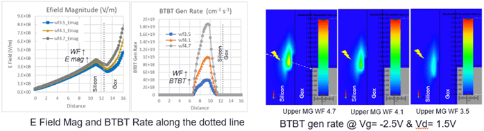
Fig. 5: Electric field and BTBT rate at the gate-drain overlap region (left) and a 2D field view of BTBT rate at Vg=-2.5V and Vd=+1.5V bias conditions (right).

Fig. 6: Id vs. Vg in linear regime @Vd=0.1V (left), Id vs. Vg in saturation regime @ Vd=1.5V (middle), and Isub vs. Vg @Vd=1.5V (right).

Fig. 7: Isub and max BTBT rate vs. gate oxide thickness (left) and Isub and max BTBT rate vs. source/drain doping (right).
Performing device electrical analysis during process integration modeling can enable the following types of advanced analyses that identify design-technology trade-offs:
The dual work-function metal gate (DWMG) is a robust, scalable solution for mitigating GIDL in DRAM technology. By optimizing the electric field distribution, this design effectively reduces leakage currents while maintaining critical IV performance. Process integration modeling combined with electrical analysis capabilities is instrumental in demonstrating the ability to reduce leakage current using DWMG, offering a comprehensive framework for addressing design and integration challenges.
Future research efforts could include:
 |
 |
 |
|
 |
 |
 | |
Leave a Reply