Investigate and predict early electrical performance to drive package development and selection.

By Keith Felton and Cristina Somma
With the massive growth of electronics in the automotive sector (such as autonomous driving, electric vehicles, and safety systems), the complexity, capabilities, and volume of semiconductors is rapidly increasing the demand for greater package connectivity density.
This has led to high-end IC-package solutions, such as copper pillar bumping with very fine pitches for flip chip applications. Furthermore, the move towards more in-package silicon integration using complex configurations and the requirement to improve substrate stack-up with an increasing number of metal layers to meet performance specifications make configurations and system iterations much more complex.
Within this context, the approach to design must include an in-depth assessment, starting with early-stage feasibility analysis, to investigate and predict early electrical performance in order to drive package development, selection, and technology.
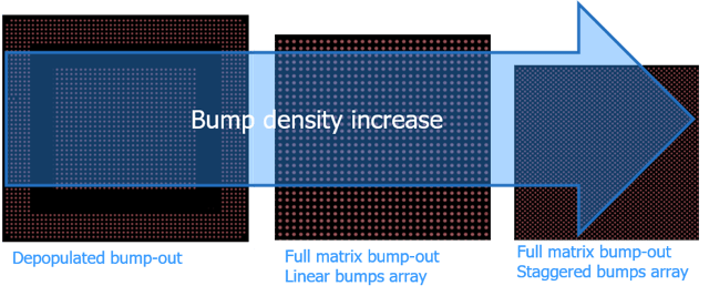
Advanced driver-assistance systems (ADAS) are pervasive today in almost all new vehicles on the market, and their level of capabilities continues to increase, requiring higher semiconductor integration, performance, and bandwidth while producing smaller overall device form factors. Figure 1 shows an example of bump-out evolution for automotive applications.

Fig. 1: Bump-out evolution for automotive applications.
The impact on package design is considerable, including, but not limited to, the design trends shown in the table.
To support automotive product development, a package design flow must be well-structured across each of the three macro stages described below.
Here the focus is on design rules identification, implementation technology, cost optimization, and design strategy validation. In this stage the design team explores through prototyping and planning the package dimension, design technology, and substrate stack-up definition. Specific areas of investigation include bump and ball out definition, breakout strategies and preliminary connectivity assignment, innovative techniques for ensuring specification uniformity, and trial or preliminary implementation for detailed performance and cost estimation.
This stage focuses on physical design, debugging, and optimization. The main activities are around substrate routing finalization and optimization, manufacturability readiness, early assessment of critical interfaces, and modeling and optimization of specific power demand—such as core supply DC drop—to prepare the design for the finalization stage and reduce overall validation cycle time.
In this last stage the focus is on electrical/thermal performance and manufacturability verification. Activities include comparison against signal integrity and power integrity target values, system-level power integrity analysis, final manufacturing verification and signoff, and, finally, tape-out handoff to manufacturing.
All three of these design stages have a fundamental dependency for co-design, co-simulation, and co-optimization at the system level, which means, in this context, at the entire device assembly level. To support this approach for automotive, high-end design, there must be a transition from a component-level to a system-level focus that incorporates die, package, and system PCB. A system-level approach enables optimization of system connectivity and performance through the usage of co-design and co-simulation techniques.
In a robust co-design flow, the handling of complex device data as designs evolve is supported by an efficient automation solution that allows more flexible feasibility analysis. The key to evaluation is the ability to integrate a prototyping tool into the current package design flow to facilitate communication across design teams. It needs to be flexible in data management and allow designers to create devices or components from scratch with the flexibility to handle complex bump and ball pitch and positions. It should also provide routing optimization and optimization capabilities for supporting fast connectivity updates and reuse of any specifications on the current or next design. Other evaluation “nice-to-haves” include the support of a systems approach as well as tight integration with layout tools that support bidirectional routing optimization.
ST evaluated the Siemens Xpedition Substrate Integrator (xSI) and found that it could address their early-stage issues and provide a solution for their co-design requirements. Among other things, xSI allows designers to quickly create and evaluate ball and bump pattern scenarios, and it provides the capabilities to plan, manage, optimize, and visualize the entire system-level connectivity from die to package to system PCBs.

Fig. 2: A typical automotive heterogeneous package assembly.
xSI allows system netlist construction and management for heterogeneous packages, aggregation of data from multiple sources in multiple formats, and visualization and interaction of all interconnect levels from a single environment. It provides hierarchical construction of the complete package assembly with step-by-step handling of multiple parts, including reuse of parts.
Based on high-speed interface connectivity planning and optimization and multi-pitch bump-out evaluation, xSI provides:
For these reasons, the STMicroelectronics Back-End Manufacturing Technology R&D located in Agrate, Italy, selected xSI to support connectivity optimization in their next high-end automotive co-design project.
In the Siemens EDA whitepaper “Methodology and Process for Heterogeneous Automotive Package Design,” we share more about this solution and why we adopted it, including best design practices and our evaluation test case. Download it here for more insights into how you can begin designing tomorrow’s heterogenous automotive package designs today.
Keith Felton is product marketing manager for High Density Advanced Packaging at Siemens EDA.
Cristina Somma is a package development senior engineer at STMicroelectronics.
Leave a Reply