Being able to put together stacks of thinned die without worrying about TSVs is a potentially huge benefit.

Hot Chips 26 wrapped up this week and there were many interesting presentations. One of the many presentations that caught my attention was given by Dave Ditzel, CEO of ThruChip, and is titled, “Low-Cost 3D Chip Stacking with ThruChip Wireless.” The technology is as it sounds — a wireless communication path for stacked die.
The first question you may be asking is, ‘Why would anyone want to do that?’ The simple answer is cost. Dave showed that the cost for using through-silicon vias (TSVs) is 1.4x to 2x over bare die. TSVs require a new CMOS process along with incurring an area impact from the TSV and its associated Keep Out Zone (KOZ), a region where no transistors are placed because of the stresses induced by the TSV that can impact transistor performance. Of course, TSVs do have the benefits of lower per bit I/O energy along with creating the opportunity for thousands of I/O compared to wire bonded connections. What if it were possible to get those benefits and more without the high cost, but how?
As the title implies, a wireless link is used to provide a communication path between chips. In order for this to be practical it needs to be a low-power, low-cost solution and have good scalability. The communication links are created by metal loops that form small inductors, and by running a current through the loops a magnetic field is generated that can be used to induce a current in another inductive loop on an adjacent chip. Figure 1 below shows a possible implementation using metal2 and metal3 layers to form the loops. At 1D spacing, the cross coupling is negligible. The loop diameter needs to be about 3x the vertical distance when stacked.

Figure 1. Example Inductive Metal Loops with 1D Spacing
Figure 2 shows the bandwidth available vs. the communication distance using a loop diameter that follows the 3x stacked distance rule. The assumed die-pitch is 8μm.

Figure 2. Useable Bandwidth vs. Communication Distance
The next question may be, ‘8μm die pitch?’ Yes. Perhaps the true enabling technology here is the ability to back grind die to 8μ (or less) in thickness. The industry state of the art has been the ability to back-grind a 700 to 800 μm thick wafer to about 40 to 50 μm. DISCO Corp. is now able to thin wafers using a “Gettering Dry Polish” wheel, which forms gettering sites while grinding. That allows thinning of wafer silicon to a few microns without device damage.[1] In a paper on ultra-thinning down to 4 μm, it was concluded there was “no degradation in terms of retention characteristics, and distribution employing 2 Gb DRAM wafer was found after ultra-thinning.”[2] This technology enables the die to be stacked much closer together and the coils to have a smaller diameter.
In order to further increase the density of the coils compared with Figure 1 above, Quadrature Phase Division Multiplexing (QPDM) can be used to pack them, as is shown in Figure 3 below. Another advantage of this technique is that inductive coupling actually gets better as the die get thinner, and it’s well understood and has been validated by dozens of test chips.
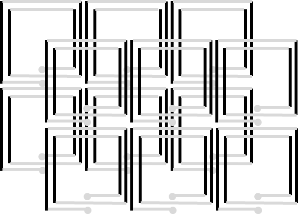
Figure 3. Denser Coil Packing Enabled by Using QPDM
So what are the projected gains from this proposed technique? Figure 4 shows an example comparison for a stack of 16 NAND Flash die. The Z-height decreases significantly from ~1000 μm to ~80 μm and the I/O energy per bit is less than 1/400th as much compared to a stacked wire bonded approach.
Wireless:
NAND

Slide 7
Figure 4. NAND Wirebond vs. NAND Wireless
In the case of stacked DRAM die, as shown in Figure 5, the vertical dimension goes from ~275 μm to ~40 μm and the I/O energy per bit is less than 1/10th as much.

Figure 5. DRAM TSV vs. DRAM Wireless
The above two examples make the technology look pretty compelling. Getting heat out of the stack woud appear to be a challenge and it will be interesting to see how this technology progesses in the near future. Dave also described a technique for using highly doped silicon to provide vertical power distribution routes throughout the stack. At
[1] “Introduction of Gettering DP Wheel”, DISCO Website, in both English and Japanese, http://www.disco.co.jp/jp/solution/apexp/polisher/gettering.html
[2] Y.S. Kim, et al., “Ultra Thinning down to 4µm using 300-mm Wafer proven by 40-nm Node 2 Gb DRAM for 3D Multi-stack WOW Applications”, Symp. VLSI Circuits, pp. 22-23, June 2014.
[3] A.R. Junaidi, Y. Take, T. Kuroda, “A 352 Gb/s Inductive-Coupling DRAM/SoC Interfaces Using Overlapping Coils with Phase Division Multiplexing and Ultra-Thin Fan-Out Wafer Level Package”, Symp. VLSI Circuits, June 2014.
 |
|
 |
 |
 |  |
 |  |
Regarding Figure 5: I think your TSV example must be HBM or HMC, correct? Using TSV does NOT necessarily cause a stack to be that high. The Tezzaron five-die DRAM stack (with TSV) looks a lot like the wireless example in Figure 5.
finally one more ( after APSTL Magic Chip ) electrical solution to an electrical problem ( bandwidth & data ), even though there is that bit about I/O pitch having to be > 3x of total stack ht., but it still beats the Popular Mechanics approach of TSVs oversold by non – technical bloggers, even various technical people in Govt. funded European Labs who should have known better but swept under the rug critical thermo – mechanical challenges with stacking thinned wafers with Cu filled TSVs ( warpage, handling, bond / debond, breakage ), after stacking TSV stress on device ( KOZ ) !