Understanding SRAM is key to understanding the effects of various memory operations on a power grid.

Introduction
Due to the overwhelming technical advantages of having on-chip memories, embedded memories are ubiquitous in most chip designs, and can comprise significant portions of a chip (upwards of 50%, according to some authors).
Accordingly, a chip’s power grid design and analysis must account for the impact of these embedded memories, but design teams often struggle to resolve power issues related to memory blocks. The good news is that it doesn’t have to be that hard—a little knowledge goes a long way.
Since memory design requires specialized transistor-level circuit design and layout expertise, embedded memory blocks are built by either a third-party provider or a separate memory design group. The memory block is delivered as a package with various design views, along with highly abstracted timing and power grid specifications (memory data sheet). Many design and verification groups tasked with using or verifying memory blocks have an incomplete understanding of these internal operations, so they treat embedded memories as a monolithic blackbox.
However, when issues arise, accurate interpretation of those abstracted specifications requires an awareness of the basic internal operations of these memory blocks. Without this knowledge, it is understandable why issues involving memory blocks are a source of frustration for many design teams.
In reality, it is not difficult to understand the internal operations of a memory block, which is basically a finite state machine with a limited number of state transition trajectories. A fundamental knowledge of these state transitions is especially important during dynamic power grid analysis, because there are spatial and temporal aspects that must be considered. Different regions of a memory block interact with the power grid at different times, based on active memory micro-operations.
My goal here is to present an overview (or review) of the internal operation of an embedded static RAM (SRAM) memory that provides you with the essential knowledge you need to interpret a memory data sheet with regard to the impact on a power grid. I won’t go into the gritty technical details (if you want more in-depth technical details, check out the suggested reading at the end). I’m concentrating on SRAM, rather than other memory structures, since it is compatible with the standard logic process.
SRAM Memory Architecture
Let’s start with a description of the basic components of a typical memory architecture, and discuss the rationale for design consideration that motivates some of the architecture decisions. This working knowledge about typical SRAM memory architectures is necessary for understanding memory block internal operations.
Sub-blocks
Typical SRAM memory architecture consists of the following sub-blocks (Figure 1).

Figure 1. Memory sub-blocks of a SRAM architecture
A bitcell is implemented as a minimally-sized cross-coupled inverter with an n-type mosfet (NMOS) pass transistor that provides external access to the cell state (Figure 2). The basic bitcell configuration takes six transistors (6-T), although there are other implementations, such as five transistors.

Figure 2. Memory bitcell views
A memory organized as M words consisting of length N-bits has a bitcell array containing M rows of N columns of bitcells. There is a pair of lines (bitlines) associated with each bitcell column. All the bitcells within a given column in the bitcell array are connected to the bitlines in the same column, so the sense amp circuitry can be reused for multiple word addresses (Figure 3). For example, the bitcell in column 0 is connected to the 0th column bitlines (positive and negative polarity), and likewise, the bitcell in column ith is connected to the ith column bitlines.

Figure 3. Bitlines
Column Drivers and Sense Amplifier
As shown in Figure 3, a bitcell line has a relative large parasitic capacitance, derived from both the long metal run spanning all the array rows and the diffusion capacitances from the NMOS pass devices. This large bitline capacitance presents two issues that can impact design.
First, a bitcell PMOS transistor must be significantly larger than minimum transistor width to have sufficient current to drive a bitline to a high logic value (as shown in the Figure 2 transistor view). This is because a PMOS transistor must have roughly twice the width of an NMOS transistor to have the same current drive due to the difference between hole and electron mobilities. This increased sizing is a concern, since the bitcell layout area directly impacts the memory block layout area, and it is generally advantageous to use minimally sized transistors to achieve area reduction.
To avoid requiring large PMOS transistors in the bitcell, the bitlines are typically pre-charged to either Vdd or Vdd/2, so that only NMOS transistors in the inverters are required to sink appreciable current during a discharge of the bitline. The large PMOS transistor required to charge a bitline to logic HIGH resides in the Column Driver sub-block, rather than being in each bitcell. This placement allows the big PMOS transistor overhead to be amortized among the bitcells associated with the column. The alternative would be to have the large PMOS transistor in each of the M x N bitcell. For example, in a 128-word by 32-bit memory block, this would require the layout area to accommodate 8192 large PMOS transistors (2 PMOS/bitcell * 4096 bitcells), whereas the Column Driver approach requires just 64 (32 d and 32 inverted d bitlines) large PMOS transistors.
Second, a bitcell state can be inadvertently corrupted during a read operation, due to the large charge stored on the bit line. One technique to avoid this corruption is to not require the bitlines to have full voltage logic swing prior to detecting the correct logic value in a bitcell. To this end, the sense amp circuitry can resolve the bitcell state by small voltage differences (differential input) between the bit and bit bar (inverted). Figure 4 shows a transistor-level implementation of a differential input sense amp. There are other sense amp implementations that require a single bitline, rather than a differential pair, and result in an area saving due to the elimination of half of the bitlines—however, there are performance tradeoffs for the area savings that must be taken into account when making this design decision.

Figure 4. Differential Input Sense Amplifier
Multiple Bank Configurations
Ultimately, there is a maximum bitline capacitance value that a minimally-sized bitcell can accommodate, and still have acceptable performance. To allow memory sizes beyond this limit, one technique is to reduce the array row size by using multiple banks of memory arrays. In a two-bank architecture, each bank has half the bitline capacitance compared with the single bank configuration (Figure 5). A four-bank configuration has one-quarter the bitline capacitance in each bank.

Figure 5. A two-bank memory configuration reduces the capacitance in each bank, compared to a single bank configuration.
SRAM Memory Operation
Next, let’s look at several memory micro-operations, and the sub-blocks that are active during these operations. By deducing where the sub-blocks are located in the memory block, designers should be able to localize when and where the power grid is being exercised. Figure 6 shows a four-bank memory layout with some sub-blocks identified.
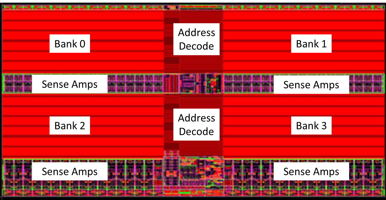
Figure 6. Four-bank memory with sub-blocks
Memory Write
During the memory write operation, new data are written into the bitcell array. Conceptually, the steps involved are (Figure 7):

Figure 7. Memory Write micro-operations
Figure 8 shows the power activity levels of sub-blocks (either drawing or pushing current) in the power grid during the various steps of the write operation.

Figure 8. Power activity levels during Write operation
Memory Read
A memory read operation performs the following steps (Figure 9):

Figure 9. Memory Read micro-operations
Figure 10 (below) shows the power activity levels of sub-blocks (either drawing or pushing current) in the power grid during the various steps of the Read operation.

Power-Saving Modes
The goal of a power-saving mode is to lower the power usage during times when the memory is either inactive or not being used. Since most of the quiescent (idle) power is a by-product of leakage currents, almost all power-saving techniques target the reduction or elimination of this leakage current. The most straightforward approach is to turn off unused sub-blocks by using power gating. Retention mode preserves the memory state by various means, such as raising the bitcell threshold voltage, or lowering the voltage to the so called minimum data retention value (DRV).

Figure 11. Memory power modes
Typical memory power modes (Figure 11) include variants of the following:
From a power grid perspective, the most interesting modes involve transitions from a power-off state (power-down) to an on-state (power-up) mode, because there will be a current surge or in-rush current as effective capacitances are being charged.
The worst case is from shutdown mode to normal mode.
Summary
Having a general awareness of an embedded SRAM memory architecture is key to understanding the effects of various memory operations on a power grid. Almost all SRAM blocks are derived from the same generic template, so once you grasp the basics, it is easy to infer how your particular memory variant will behave. This knowledge is especially important during dynamic power grid analysis, when different sub-blocks are actively stressing the power grid at the various micro-operation steps. It is crucial that your power grid analysis tool captures these memory micro-operation sequences correctly to ensure the spatial and temporal effects are accurately identified and understood.
Additional Reading
Clark, L.T.; Morrow, M.; Brown, W., “Reverse-body bias and supply collapse for low effective standby power,” Very Large Scale Integration (VLSI) Systems, IEEE Transactions on , vol.12, no.9, pp.947,956, Sept. 2004
doi: 10.1109/TVLSI.2004.832930
URL: http://ieeexplore.ieee.org/stamp/stamp.jsp?tp=&arnumber=1327631&isnumber=29361
Dehaene, W.; Cosemans, S.; Vignon, A.; Catthoor, F.; Geens, P., “Embedded SRAM design in deep deep submicron technologies,” Solid State Circuits Conference, 2007. ESSCIRC 2007. 33rd European, pp.384, 391, 11-13 Sept. 2007
doi: 10.1109/ESSCIRC.2007.4430324
URL: http://ieeexplore.ieee.org/stamp/stamp.jsp?tp=&arnumber=4430324&isnumber=4430237
Gries, Matthias. A Survey of Synchronous RAM Architectures. Zürich: Computer Engineering and Networks Laboratory (TIK), Swiss Federal Institute of Technology Zürich (ETH), 1999.
Nakadai, Hiroshi, Gaku Ito, and Toshiyuki Uetake. “Embedded SRAM Technology for High-End Processors.” Fujitsu Science Technology Journal 47.2 (2011): 150-56.
Sharifkhani, Mohammad, and Manoj Sachdev. “Segmented Virtual Ground Architecture for Low-Power Embedded SRAM.” IEEE Transactions on Very Large Scale Integration (VLSI) Systems 15.2 (2007): 196-205.
Pavlov, Andrei. Design and Test of Embedded SRAMs. PhD Thesis, University of Waterloo, 2005.
Qazi, Masood, Mahmut Sinangil, and Anantha Chandrakasan. “Challenges and Directions for Low-Voltage SRAM.” IEEE Design & Test of Computers (2010), pp. 32-43.
Qin,H. et al., “SRAM leakage suppression by minimizing standby supply voltage,” Proceedings ISQED, pp. 55-60, 2004.
Yabuuchi, Makoto, et al., “A 45nm Low-Standby-Power Embedded SRAM with Improved Immunity Against Process and Temperature Variations.” Solid-State Circuits Conference, (2007): 326-327.
Yamaoka, Masano, et al., “A 300 MHZ 25uA/Mb Leakage On-Chip SRAM Module Featuring Process-Variation Immunity and Low-Leakage-Active Mode for Mobile-Phone Application Processor,” “Solid-State Circuits Conference, (2004).
 |
|
 |
 |
 |
 |
 |
 |
 |
 |
Leave a Reply