Prevent critical failures caused by overcurrent-induced fusing.

Copper (Cu) redistribution layer (RDL) technology is used to interconnect chips in various high current Wafer Level Packaging (WLP) applications. Typically, Cu RDLs with thicknesses of 5-9 µm and widths of 5-20 µm are used for high current sourcing. In this case, the temperature of the Cu RDL metal line increases due to the Joule heat generated when current passes through the metal line. If an unexpected overcurrent is applied, fusing occurs due to the Joule heat exceeding the melting point (1086°C) of the copper. This overcurrent-induced fusing is a critical failure mode for electronic devices.
Because of these considerations, the study of fusing current has been conducted since the 1880s. However, there has been minimal research in recent decades, except for some issues related to printed circuit board (PCB) traces and wires [1-4]. Representative papers on fusing currents typically depend on two studies. One is a study by Onderdonk published as long ago as 1944, and the other is an older study by W. H. Preece published in the 1880s [5-6]. Both studies are limited to fusing current in wires. Data on theoretical studies and experimental work on WLP either does not exist or is rarely cited.
In this blog post, empirical data obtained through fusing current experiments is used to predict the fusing performance by data extrapolation. By correlating with thermal simulations to validate real-world fusing performance, it provides reliable data on fusing current performance for different RDL designs and structures.
The WLP made for Cu RDL fusing testing had a die size of 9.6 mm x 9.5 mm. Fabricated in a 5×2 array for convenience in handling and testing, its total size was 48.00 mm x 19.00 mm. The WLP test vehicle (TV) consists of a thick Si die with a 0.5 µm thick silicon nitride passivation and a 5 µm thick polyimide was applied as dielectric material to surround the Cu RDLs. Unlike a typical Chip Scale Package, no leads (CSPnl), ball grid array (BGA) balls and under-bump metallization (UBMs) are excluded. Also, the probing pad is made of a large area Cu pad of 500 µm x 350 µm instead of a BGA balls to withstand high Joule heating during testing. The overall package structure is shown in figure 1.
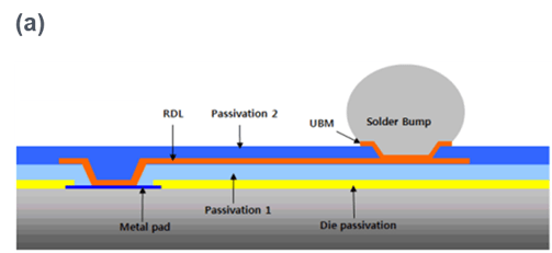

Fig. 1: (a) Cross-sectional image of a typical CSPnl and (b) cross-sectional and top view image of the test vehicle.
The Cu RDL was plated with various RDL designs (5~20 µm width, 5~9 µm thickness and short~long length), patterns (straight, two-corner and four-corner) and Si die thickness (thin~thick). Table 1 and figure 2 show the design of experiments (DOE) and schematic illustration of the tested Cu RDL design.
| Thickness [um] | 5 | |||
| Width [um] | 5 | 10 | 15 | 20 |
| Length [um] | Short, middle and long | |||
| A [um2] | 25 | 50 | 65 | 100 |
| Thickness [um] | 9 | |||
| Width [um] | 5 | 10 | 15 | 20 |
| Length [um] | Short, middle and long | |||
| A [um2] | 45 | 90 | 135 | 180 |
Table 1: The DOE matrix of the manufactured Cu RDL.

Fig. 2: (a) Cu RDL patterns for fusing testing and (b) top view of Cu RDL in various plated patterns.
Figure 3 shows the evaluation results of the fusing currents. The evaluation was performed using a source measure unit (SMU). In addition to the different RDL designs, various silicon thicknesses were evaluated to observe fusing performance as a function of silicon thickness.
Figure 3 (a) shows the fusing test results for the short length of Cu RDL. For a cross-sectional area of 178.9 µm2 (20.8 µm width and 8.6 µm thickness) and thick silicon thickness, the fusing performance was 306% higher than the cross-sectional area of 18.5 µm2 (4.3 µm width and 4.3 µm thickness). Since resistance is inversely proportional to cross-sectional area, as the cross-sectional area increases, the resistance decreases and current is proportional to the cross-sectional area, so as the cross-sectional area increases, the current value also increases.
For a cross-sectional area of 178.9 µm2, it showed 42% higher fusing performance when the Si thickness was thicker than when it was thinner. This shows that the silicon is very effective for dissipating the Joule heat generated by the RDL. In particular, the structure of the test vehicle is more effective in terms of heat dissipation because the silicon is located directly under the RDL. However, the cross-sectional area of 18.5 µm2 showed 6.7% higher fusing performance even though the Si thickness was increased. For a smaller cross-sectional area, the difference in performance based on Si thickness was not as large as expected. As the thickness of the Si increases, it should have better performance in terms of heat dissipation. However, the smaller cross-sectional area has a higher resistance, which means relatively more Joule heat. For this reason, there was much more heat increasing due to high resistance than heat dissipated by Si in the small cross-sectional area.
Figure 3 (b), (c) shows the fusing performance for Cu RDLs of middle and long lengths, respectively. For cross-sectional area of 178.9 µm2 and thick Si thickness, it showed 25% lower fusing performance when the length of Cu RDL was increased. This is because resistance increases proportionally to length.
Figure 3 (d) for the two-corner and four-corner pattern, it was thought that fusing would occur faster due to the concentration of current in the localized corner area. However, they showed the same resistance and fusing current compared to the straight pattern. The experimental approach is not to apply a constant current for a long time under steady state conditions, but to induce failure of the Cu RDL in a relatively short time by repeatedly applying a high current at specific times. As a result, it was difficult to see the differences between the patterns because there was not enough time during the seconds-long test for any electromigration or damage to the trace to occur at the current density concentrations at the corners.
Based on the experimental data obtained from the performance evaluations, a cubic equation was created through data extrapolation. Thus, by entering the required cross-sectional area in the variable ‘X’ in each term, the fusing current can be calculated based on the length, Si thickness and pattern. In figure 3, the dotted data is the experimental value, and the line data is the calculated value from the cubic equation. Both calculated and experimental values showed excellent correlation and matched very well.

Fig. 3: Evaluation results of the fusing current, (a) Cu RDL with straight pattern of short length (b) Cu RDL with straight pattern of middle length (c) Cu RDL with straight pattern of long length (d) Cu RDL with two and four-corner pattern of long length.
Finite Element Analysis simulation was used to verify and validate the experimental results reported in this paper. Ansys Mechanical 2022 R1 was used for all simulation of the fusing current experiment. Simulation work is very helpful for determining the sensitivity of variables with the small and delicate trace structures and the fusing process caused by Joule heating.
Fusing occurs when the thermal energy produced within an electrical conductor exceeds the system’s ability to absorb that energy and the surrounding environment’s capacity to remove that energy. When this occurs, the conductor is heated until it experiences some failure of integrity such as vaporization (at very high currents and very, very short time scales) or melting that leads to segmentation or breaking of the conductor (for gradually ramped or sustained currents and longer time scales). For this experiment, fusing is not an instantaneous process nor is it a steady-state process; therefore, transient simulation (where the time domain is considered) must be performed. The key factors that must be included in this model are a) time and test current applied over time, b) trace (conductor) cross-sectional area, length and material resistivity, c) thermal conductivity and heat capacity of the materials in the system, d) size and mass of the primary bodies of the system and e) heat transfer out of the system into the environment through radiation and convection.
Ansys Workbench has a “Thermal-Electric” coupled analysis system using the Mechanical APDL solver that is appropriate to use for this simulation.
A small heat transfer coefficient was applied to all external surfaces of the model to account for cooling via convection and radiation. The primary path of heat transfer away from the trace is through conduction into the silicon die below the trace, so the exact value of the surface heat transfer coefficient is not very critical to the model. Most of the heat is absorbed by the die itself during the duration of the test (typically less than 30 seconds) and not the surrounding air or environment. In the experiment, current was delivered to the trace through tungsten tipped probes. These probes were represented in the simulation model. Their exact dimensions, location and orientation were assumed to not be critical to the model result, but heating at the contact was observed between the probe and pads that was deemed necessary to include in the model due to the proximity of the pad, probe and trace. Tungsten material properties were sourced from existing data [7]. The model and mesh of one example are shown in figure 4.

Fig. 4: Model example showing middle length x 20.8 µm x 8.6 µm trace on a thick die. Simulation setup and labels on key bodies in the model.
The simulation is driven by setting the top surface of one probe body to be ground (0 Volts) and using an MAPDL code snippet to increase the current by discrete steps at regular time intervals at the top surface of the other probe. The simulation ends and fusing time and current are reported when the maximum temperature of the trace body exceeds the melting point of copper.
The simulation set was run, and results are reported in figure 5. A resulting plot was selected as a discussion example from the middle length x 20.8 µm x 8.6 µm trace on a thick die. The figure shows the time step when the peak temperature in the model exceeded 1086°C. It was noted that the center of the trace length shows the highest temperature, which aligns well with observation of the real-world experiment. The pads on either end of the trace appear to be several hundred degrees cooler, and the bulk of the die remains much cooler than the trace region. This figure demonstrates the significant temperature gradient experienced by the system and the importance of the heat capacity of the thick die.

Fig. 5: Model example showing middle length x 20.8 µm x 8.6 µm trace on a thick die. The full die and trace (top). Simulation setup and labels on key bodies in the model (bottom).
The simulation results for long length of Cu RDL compared to the real-world experimental measurements are shown in figure 6.

Fig. 6: Simulation results plotted with measurement results for the full simulation data set.
In this study, fusing current evaluation and simulation were performed for various designs (5~20 µm width, 5~9 µm thickness and short~long length), patterns (straight, two-corner and four-corner), and various Si die thicknesses. The fusing current was not only a function of the area of the Cu RDL, but also the heat dissipation by the package structure. In this evaluation, a cross-sectional area of 178.9 µm2 showed 42% higher fusing performance when the Si thickness was thicker than when it was thinner. The conclusion is that the silicon is very effective for dissipating the Joule heat generated by the RDL. In particular, the WLPs test vehicle structure is more effective in terms of heat dissipation because the silicon is located directly under the RDL. Based on these experimental data, a cubic equation was created using data extrapolation, that allowed the calculation of fusing current values that matched the actual results very well.
Simulation aligns with the experiment measurements presented in this paper and correlates well with the trends and data. Fusing current simulation results were very close to the measured fusing current and trends were well aligned with R values of 0.99. This validates the simulation approach and methodology used in this paper. The die thickness appears to have a much larger impact on fusing current magnitude in simulations than in the real-world experiment.
 |
 |
 |
|
 |
 |
 | |
 |
Leave a Reply