Small, densely packed features in interposers mean electromagnetic effects can be exceptionally consequential.

By Matt Commens, Juliano Mologni, and Pete Gasperini
Today’s 3D integrated circuit (3D-IC) technology is the culmination of 40 years of research in universities and laboratories scattered across the globe. Beginning with dynamic random-access memory (DRAM) deployments that appeared on the market a decade ago, 3D-IC has since expanded its reach. It is now decisively beginning to achieve the continuation of Moore’s Law by other means: providing greater functionality and performance in the same or smaller footprint. A key element in the technology is the interposer, which provides the mechanical means to stack die while facilitating their vertical interconnection schemes without impinging upon performance.

Fig. 1: 3D-IC device on a PCB.
It would be a mischaracterization to dismiss the interposer as simply a package substrate moved into the vertical dimension. Interposers are complex structures with multiple layers – separate power and ground routing nets, along with TSVs (thru-silicon vias) with liners. All of these features are incorporated into proven IC manufacturing processes.
Interposer analysis challenges to consider
There are some important factors to consider when assessing aspects of interposers. A marked difference between conventional organic package substrates and interposers is that the latter support elements in much finer dimensions and in greater detail which can be virtuous when packing more functionality onto the same footprint. However, when features are quite small and densely packed, multi-physics electrical and thermal effects can be exceptionally consequential. Frequency dependent effects in the materials can create significant coupling risks. The substrate itself, composed of silicon, also tends to be somewhat lossy. Due to these circumstances, interposers can in effect conceptually be treated as a package development that uses an IC process.
As a residual of the above, interposers manifest the same potential sources of problems that are observed at the organic package and PCB level with regards to signal and power integrity. The incorporation of signaling and power distribution networks in the interposer are primarily intended to forestall electromagnetic interference (EMI) and parasitics – a particular bane of the kinds of high-performance designs that employ 3D-IC packaging.
An example of 3D-IC and the critical role of interposers is the implementation of a general purpose high-performance CPU with its supporting instruction and data memory architecture (see Figure 2 below.) The SerDes chip-to-chip connections and high bandwidth memory (HBM) 2/3 for core to memory I/O for L0-L4 data and instruction caches are rendered maximally effective by chiplet stacking with high functionality interposers.

Fig. 2: Multi-chiplet CPU design.
But 3D-IC packaging technology, though offering tremendous possibilities for the microchip sector, has suffered from inadequacies in support from electronic design automation (EDA) electromagnetic simulation software. Most tools do what they can with a detailed GDS level of inputs and strive to achieve some moderate level of performance and accuracy. These offerings, however, struggle to execute simulations at this scale of complexity employing (at times hidden) simplifications or behind-the-scenes divide-and-conquer techniques, which take many time-consuming iterations before a solution reaches even marginal acceptability.
Achieve system-level, scalable, and optimized 3D-IC EM simulation
It is essential to come to terms with the reality that 3D-IC is one of the most difficult EM simulation problems to solve today. This is a repercussion from the rapid advancement of 3D-IC hardware, with its resultant sophistication outpacing the ability of many EM software simulators to properly support it. For an EDA offering to be capable of rising to the occasion, it must meet the following criteria:
What is needed is a solution that is system-level, highly scalable, and capable of optimizing across multiple design parameters.
The approach offered by Ansys includes a foundational model of an interposer with a base set of design parameters used in conjunction with Ansys HFSS electromagnetic simulation software and Ansys optiSLang optimization software. The intricacy of the simulation problem requires this multifaceted approach, as we detail below.
The model itself consists of an interposer with a 300nm silicon dioxide substrate, complete with two die on top, power and ground nets and an array of TSVs. The frequency sweep ranges from 0-40GHz with an adaptive frequency set at 10GHz. A graphical depiction is provided in Figure 3 below.

Fig. 3: A CAD representation of a basic interposer model.
The model is adaptable to support additional features such as decoupling capacitors. It can also be incorporated into a simulation extended to encompass the full package, as well as the PCB using HFSS (more on that below).
The scalability of HFSS is critical to properly simulating the interposer. The scalable elastic solver technology of HFSS enables a single system to be solved without compromise across networked machines, thus not requiring the use of a single and large shared memory workstation. HFSS scales from micro to macro, so it can solve models assembled from fused meshes that have been adapted to the geometry and the electromagnetics and scaled from 3D-IC to packages, PCBs to routers, and servers to ships, literally from chips to ships.
HFSS 3D Layout captures the interposer model in all its detail and provides critical modeling and simulation support at these dimensions using a 3D finite element mesh that is adapted for accuracy. Component libraries in HFSS 3D Layout include objects such as the vias, nets, and the entire vertical assembly of features as a stackup.
Furthermore, the fundamental parametric nature of HFSS lends itself readily to simulating the basic interposer model with multiple variables. In this example, the interposer model is configured to support six variables – signal and power trace widths, the radii of the TSV and interposer bump, the interposer Vdd aperture and the diameter of the via. These can, of course, be changed or expanded as needed for a given application.
An intelligently guided iteration scheme is required to optimize the parameters. This is where optiSLang comes into the workflow. Ansys optiSLang is an AI-driven tool that creates a design of experiments from parametric criteria. It converges on the optimal solution by learning from each self-executed simulation run, learning on its own the relative importance and weight of the parameters. This leads to a more efficient path for optimizing a multivariate simulation solution. A 5x improvement in simulation time is typical when using optiSLang.

Fig. 4: A metamodel of optimal prognosis (MOP) from OptiSLang.
Both HFSS and optiSLang also support distributed computing for simulation acceleration through task parallelization, further improving simulation turnaround times.
Field post-processing is an overlooked but vital step in finalizing complex EM designs. HFSS enables designers to visually observe what happens to EM fields over a given frequency range to more clearly perceive wave propagations and their effects. An example of this with the foundational interposer model is shown below.

Fig. 5: EM wave propagation in foundational interposer model (HFSS 3D Layout).
The final step for design sign-off employs HFSS to simulate the interposer, package and PCB together in a single, fully coupled full wave simulation using HFSS Mesh Fusion.


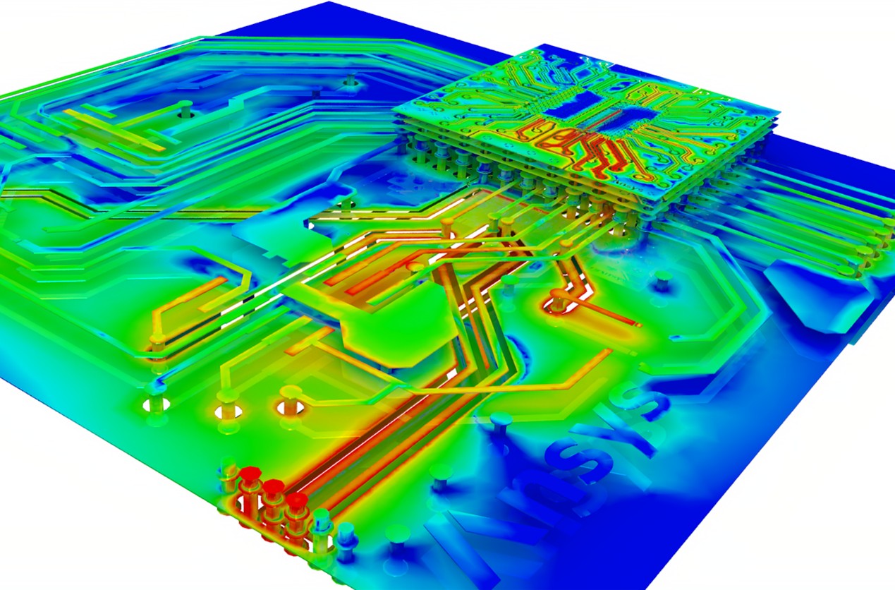
Fig. 6: Full wave mesh fused system level HFSS simulation.
Alternate approaches to interposer EM simulation have proven unsatisfactory because of their inability to scale, optimize efficiently and successfully against multiple variables, solve the EM simulation in a practical time frame and meet the full performance possibilities of the hardware. This is why Ansys implemented parametric-driven simulators with AI-instigated optimization and post processing analysis support.
Ansys is featuring this workflow at the Design Automation Conference in San Francisco July 10-14. For more information attend the presentation “Electromagnetic modeling for Signal Integrity analysis of chiplet designs” by HFSS Senior Product Manager Matt Commons at the Ansys DAC booth #1539 at 11:00, Wednesday, July 13th. Take a Leap of Certainty with Ansys at DAC. Look for much more technical information over the rest of the summer.
Juliano Mologni is a senior product manager at Ansys.
Pete Gasperini is a product marketing manager in the Electronics Business Unit at Ansys.
 |
|
 |
 |
 |  |
 |  |
Leave a Reply