The foundation for a holistic design and verification approach for power modules.

By Wilfried Wessel (Siemens EDA), Simon Liebetegger (University of Applied Sciences Darmstadt), and Florian Bauer (Siemens EDA)
Power modules are high-power switching circuits that convert DC- in AC-currents in electric vehicles, renewable energy, and many more applications. New materials [14] and device technologies [14], such as wide bandgap semiconductors, including silicon carbide (SiC) or gallium nitride (GaN) require enhanced verification methods.

Fig. 1: Power Module PI2000 Siemens EDA.
The unique switching characteristics of power modules using wide bandgap semiconductors are dominated by higher frequencies compared to silicon (Si) IGBTs. Currently, Si IGBTs operate in a frequency range of about 100 kHz. Compared to that, SiC MOSFET can operate in an MHz frequency range [21]. Additionally, the device package of a SiC MOSFET is much smaller [14] than a Si IGBT with similar electrical characteristics. This makes the verification of a power module using a simulation-driven approach essential.
Already in traditional power modules, the designer was faced with a polylemma. This means a designer can no longer predict the potential contradictory effects of a single design change. For example, a simple change in the component placement affects all domains shown in figure 2. The change may alter the homogeneous current distribution through all devices (DC behavior), and the change could modify the switching behavior for the different devices in the module (AC behavior). However, changes in the electrical domain lead to implicit changes in thermal and EMC behavior. If the static and switching of the individual devices in the package are no longer uniform, their individual power dissipation results in different device temperatures and thermal stress. This stress reduces the lifetime of the components in the package and must be avoided. Matched and optimized electrical behavior of the devices also leads to low EMC radiation.

Fig. 2: Power modules are a four-dimensional design challenge.
Since standard simulation programs are insufficient, as will be shown below, complex power modules are designed using a trial-and-error process. This results in many prototypes, which are evaluated and improved until the specifications are met. Such a hand design is based on the designer’s personal experience and is not only cost-sensitive but also time-consuming. A more systematic computer-based design approach is mandatory to address this multi-dimensional problem. This article shows how S-Parameter techniques can be utilized. The simulation helps to qualify and optimize power module designs in an early design phase. The goal is to avoid the production and measurement of many prototype modules. In some areas, power modules are analyzed using lumped elements [22]. The paper [22] shows limitations, e.g., cross-coupling of multiple devices and frequency accuracy. For this reason, S-Parameters are needed.
Before going into the full details of S-Parameters, some basic understanding of power modules is required. A power module [4] uses power devices connected in parallel to switch its output node from a high potential to Ground and VCC. The power devices are mounted and interconnected in most cases using a single copper layer on a ceramic substrate directly. This simple structure lacks a return path or reference potential to model a power module using a microstrip transmission line, as shown in figure 3.
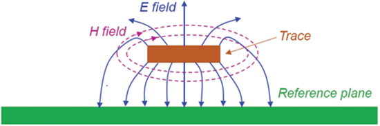
Fig. 3: Microstrip line and the surrounding fields [1].
This is why a resistance, inductance, capacitance and conductance (RLCG) parameter extraction method is currently the most common when simulating and describing power modules. Such extraction methods are widely used to extract package parasitics on ICs. The equivalent circuit of a microstrip is shown in figure 4.
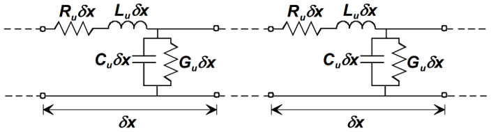
Fig. 4: Microstrip line RLCG model as through representation [2].
The circuit of figure 4 must be transformed to be suitable for power modules. Instead of a through signal description, we end up with an across-signal path in figure 5 since there is no reference potential but an insulating ceramic substrate. We see that this method of description is suitable to describe any connection between two pins as long as we do not need to consider transmission line effects [3], such as reflection and the skin effect. This is true for small structures, small compared to the wavelength lambda, which is distributed over the copper structure.
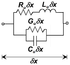
Fig. 5: Microstrip line RLCG model as across representation.
The RLCG extraction allows defining a matrix of all R, L, C and G values for a given power module. For a high current path, as shown in figure 6, this is not just a single pin-to-pin connection. Instead, multiple insulated-gate bipolar transistor (IGBT) or metal-oxide semiconductor field-effect transistor (MOSFET) are switched in parallel to share the high currents, which is to be described by a matrix of parasitics. Each location becomes a simulation port. These ports are marked in figure 6 with a red arrow. The most left port, J1, is used as a reference, and U1, U3 and U5 are signal ports. With this, the whole matrix can be calculated. A typical resistance matrix can be found in table 1.
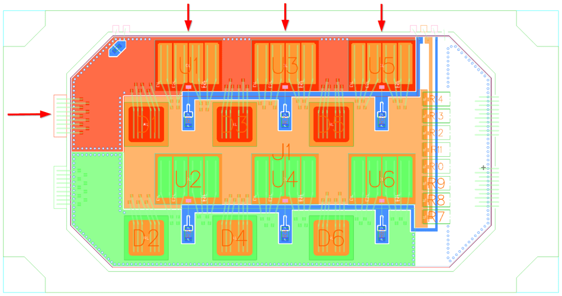
Fig. 6: Power module PI2000 Siemens EDA with marked ports.
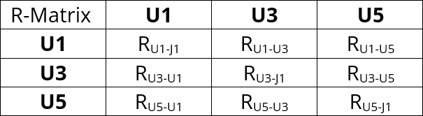
Table 1: R-Matrix for VPP net of the PI2000 power module with J1 as reference.
The table must be implemented in a SPICE netlist for a circuit simulation. The transformation of the matrix to a SPICE circuit makes things difficult. A general rule is that the SPICE circuit must be composed in the direction of the electrical current. If J1 is the enclosure terminal of the power module’s package, the current flow direction is from the IGBT U1 to J1, from U3 to J1 and from U5 to J1. These values can be found on the main diagonal of table 1. A SPICE netlist could look similar to this:
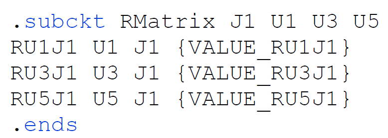
Cir. 1: SPICE circuit of the main diagonal of the R-matrix.
However, the selection of the reference pin has a huge impact on the final result. Changing, for example, the reference pin from J1 to U3 demonstrates this in more detail:
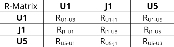
Table 2: R-Matrix for VPP net of the PI2000 power module with U3 as reference.
For the composed SPICE netlist, the resistance from J1 to U1 changed from RU1-J1 to RJ1-U3 + RU1-U3. This is physically not correct. Engineers must carefully pick reference pins in a power module verification scenario to achieve the most accurate simulation result. It is shown later that the SPICE representation has other disadvantages in the simulation performance and broadband accuracy.
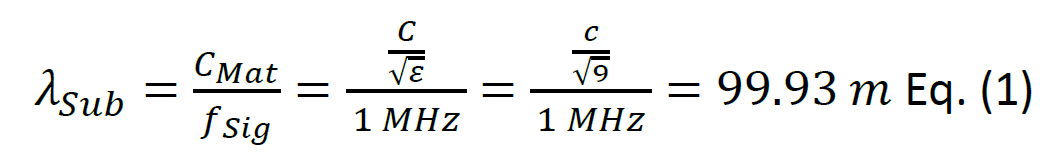
Another way to model the connection between two or more circuit nodes is using scattering parameters, or S-Parameter in a short form. S-Parameter is widely used to analyze high-speed interfaces such as peripheral component interconnect express (PCIe) or Ethernet. Based on [2],[3], an S-Parameter or an S-matrix is a mathematical concept to describe wave propagation through a multi-port network. In this definition, already one advantage and one disadvantage can be found. The advantage is that S-Parameters are capable of handling multi-port electrical networks. The disadvantage is the concept of wave propagation, which does strictly not apply in the DC range but is more suitable in the high-frequency range. Power modules based on silicon IGBTs switching frequency are far below 1 MHz. Even if harmonic frequencies are considered, it is hard to argue that wave propagation is required. Typical power modules in a performance range of 1700V and 750A, such as the Infineon FF750R17ME7D, has substrate dimension of 38mm x 100mm [4]. The wavelength of a 1 MHz signal is much bigger than this geometrical structure. Eq. (1) shows that considering a dielectric constant of a typical power module substrate, such as aluminum nitride (AlN), the wavelength is 99.93 m. An RLCG representation would be sufficient to characterize a power module based on Si devices. Looking into the future, Wide Band Gap (WBG) semiconductors such as silicon carbide (SiC) and gallium nitride (GaN) [11] are moving fast forward. These new technologies also have much higher switching frequencies and will introduce the demand for full wave effects.
There are two challenges in combination with S-Parameter simulation. Similar to the description of a microstrip, it is standard to have a reference net for each signal. As mentioned before, for power modules, this is not the case.
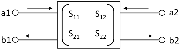
Fig. 7: Two-Port network represented as S-Parameter with reference net b and signal net a.
Figure 7 shows a two-port network. On the left side, there is pin a1 and b1, where a1 is the signal pin, and b1 is the reference pin. The same pattern can be applied to the right side. Figure 7 must be transformed for power modules to consider the missing reference net. Figure 8 shows the result of the conversion. A pin of the signal net is used as a reference pin. This method applies to power modules.
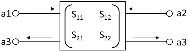
Fig. 8: Two-Port network without reference net.
Without the work described in this article, the transformed S-Parameter cannot be simulated in a circuit simulator. The reason for this is that due to the standardization for high-speed applications, all reference pins are not exported, and the pin is assumed to be connected to the reference. In the case of high-speed PCBs, this is ground or net 0. Compared to the desired situation in figure 8, the simplification is shown in figure 9. This means that with the current solution, the pin a3 does not exist in the S-Parameter. Still, it does exist for the circuit simulator. If the S-Parameter file gets back annotated to the circuit simulation, pin a3 is disconnected.
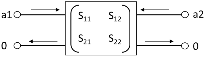
Fig. 9: Simplified two-port network model used today.
The article solves this problem and enables the usage of S-Parameter in circuit simulators like Xpedition AMS from Siemens. It also outlines the capabilities of the S-Parameter for optimization, for example, using a power module compliance check based on S-Parameter. The article does not describe how the DC behavior for S-Parameter is optimized. Modern solvers like Xpedition AMS have integrated interpolation methods to handle DC operation points.
The solution is demonstrated in the example in figure 6 for the positive supply voltage called net VPP. For the simulation of the S-Parameter and the later used RLCG matrix HyperLynx Advanced Solvers such as Fast 3D and the Hybrid solver are used [5],[20].
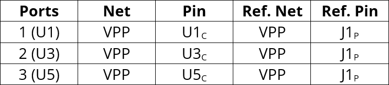
Table 3: Detailed port definition of the net VPP.
To reproduce the simulation results, the following mesh and solver settings were used:
The simulation result shown in figure 10 was expected. For a frequency between 10 kHz to approximately 1 MHz, the ohmic resistance of the copper is still dominant at higher frequencies, and the inductance path becomes dominant around 10 MHz. At higher frequencies, a resistive part, connected in parallel to the inductance, takes over (compare to figure 5). Over 100 MHz, we see additional losses, but overall this shows that the RLCG representation has a good fit at least between 10 kHz and 1 GHz. The component placement of U1, U3 and U5 in relation to J1 can explain the S-Parameter order in figure 10. Figure 6 shows that the distance between U1 and J1 is the shortest and the distance between U5 and J1 is the longest. For this reason, it is not surprising that S11 (red) have the lowest attenuation and S33 has the highest attenuation.

Fig. 10: HyperLynx Hybrid Solver simulation results for net VPP.
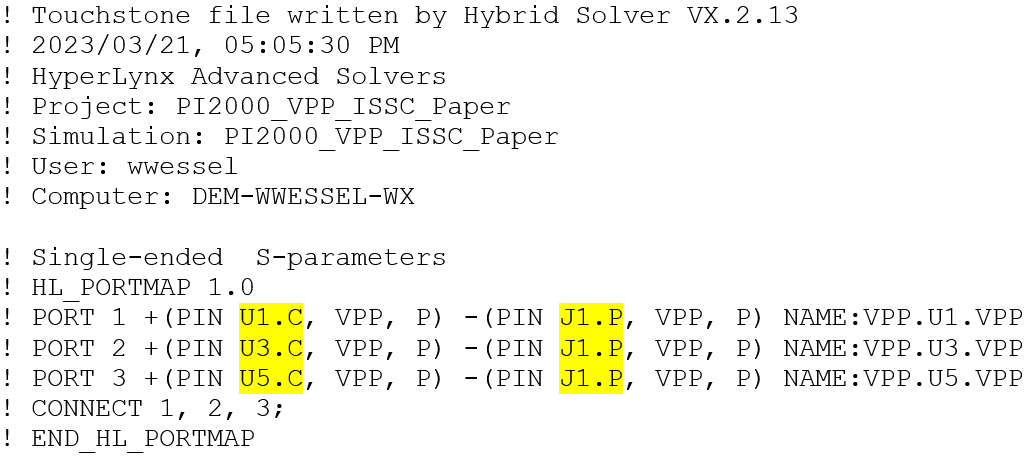
The advantage of an S-Parameter in a circuit simulation is that no transformation into a SPICE netlist is required. Compared to the RLGC, there is not only a representation of the main diagonal. Instead, the full S-matrix is available. This is important to automate the process since it is no longer required to have detailed knowledge about current paths, which was needed to select the reference pin. A SPICE wrapper file must be generated to use S-Parameter in Xpedition AMS. Line 4 in Cir. 2 shows all available pins of the SPICE subcircuit. In this line, currently, J1-P, the reference pin of table 2 is missing. In line 12, all signal and reference pins are shown. Each pin is bundled as predicted with pin 0 and not with the actual reference pin. To transform the wrapper according to figure 8, the wrapper file needs to get enhanced by the reference pin in lines 4 and 12.

Cir. 2: Standard S-Parameter wrapper file.
A subset of the transformed wrapper file is shown in Cir. 3. All required changes are marked in yellow. For a small example like this, this process is straightforward and can help to define all requirements for an automated version.

Cir. 3: Enhanced S-Parameter wrapper file.
Since the SPICE wrapper contains no information about the reference pin or pins, another source must be found. In line 13 of Cir. 2, the S-Parameter file is linked to the wrapper file. Based on the authors’ work for parasitic extraction and back annotation in 2012 [6], the header information of each S-Parameter exported by any HyperLynx products was enhanced to contain all required information. The port information is marked in Cir. 4 in yellow. Both files are ASCII files, and at least for the Siemens software environment, the information in the S-Parameter header is standardized. This is the foundation for the full automation of this process.
Cir. 4: S-Parameter header information.
For a fully automated and holistic optimization approach of power modules, relying on a single source of truth is essential. Lumped parasitics as SPICE subcircuits are standard to perform time domain functional simulation for power modules. The main reason for such a complicated approach was the missing reference plane or return current structures. Only view references like [8] were found using S-Parameter in this area, which are more suitable for power modules with their multi-port structures. This article shows the necessary steps to enhance and use S-Parameters for power module verification. Future verification methods in the electronic domain could be performed in two steps: in the first step of the process, the power module S-Parameters are extracted and compared to reference S-Parameters in a kind of compliant check. In the second step, the same set of S-Parameters is used to perform and analyze the transient time domain behavior.
The main advantage is that the same set of S-Parameter is used in frequency and time domains. This guarantees data integrity and is a fully automated process with huge advantages compared to transforming an RLCG matrix into a SPICE netlist.
Future research and work will concentrate on fully integrating S-Parameters in the engineering design environment. The integrated solution will increase acceptance in the engineering community. Only this can optimize the current design and verification process to meet the high demand for new efficient power modules in the future.
For even more on the topics introduced in this article, please download the new whitepaper from Siemens DISW, Why are S-Parameters superior for power module optimization?
Simon Liebetegger is of the University of Applied Sciences Darmstadt.
Florian Bauer is a technical marketing engineer at Siemens EDA.
References
 |
 |
 |
|
 |
|
 |
Leave a Reply