The artful balancing act of designing SoCs can no longer be accomplished with traditional RTL-to-GDSII flows.

The era of smart-everything has led to a surge in the need for semiconductor devices across a myriad of traditional and novel applications. These applications demand high performance yet energy-efficient compute over blazing-fast networks to service trillions of edge devices that are constantly consuming and generating large amounts of data. This surge has invigorated system architects to innovate architectures for optimal processing of these workloads that employ state-of-the-art machine learning algorithms. As more functionality requires packing into an already premium piece of real estate on a silicon chip, process engineers and packaging engineers are getting tasked with pushing the boundaries of physics to keep Moore’s Law ticking. The emergence of chip sizes that exceed reticle and even wafer limits on ever-shrinking process geometries, novel multi-die packaging techniques and, to some extent, even the chip shortage is testament to the market dynamics governing this insatiable need for more compute.
As system-on-chip (SoC) design teams take aim to optimize for the entire gamut of power, performance, and area (PPA), reliability, cost, and time-to-market (TTM) constraints, SoC design flows are in their crosshairs. Engineers must overcome several challenges to produce high quality, competitive products on the first production tapeout or else contend with expensive chip turns. The digital implementation flow from RTL to GDSII thus forms a linchpin that holds together these divergent design properties. This artful balancing act can no longer be accomplished with traditional RTL-to-GDSII flows employing dissociated engines that need odious manual tweaks and lengthy iterations to achieve a semblance of correlation across a multi-stage design flow as they crawl towards design targets. This leads to the advent of hyper-convergence in design flows.
Hyper-converged flows generate an optimal solution for RTL-to-GDSII by leveraging unified technology engines that share a highly scalable singular database and execute optimizations based on golden-signoff parasitics, timing, and power metrics. The capability to use all engines at any stage of the design flow on the same data model while utilizing signoff quality metrics backbone minimizes over-design related discrepancies and yields predictable design closure with no surprises late in the project.
To illustrate the importance of such flows more clearly, we can look at the evolution of achieved performance and power over time for an under-execution project’s best-database, as plotted below. A few details jump out upon closer study.
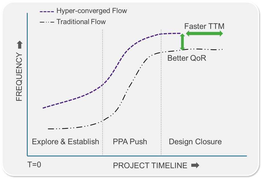

Fig. 1: Comparison of Traditional and Hyper-converged design flows.
First, there is a considerable amount of time spent by designers in the exploration phase with imperfect inputs to build a foundation for what is to come but does not really correlate to eventual PPA. This includes tasks like macro placement, special net handling, and flow pipe cleaning. Second, power usually runs wild until the later stages of the project when steps are taken, often close to signoff, to bring it under budget. While dynamic power and leakage power minimization solutions are usually employed in the PPA-push stage of the project, activity-based glitch-power usually goes unchecked until late in the project. Third, the final PPA-push and design closure steps require not only the most efficient algorithms but also the capability to quickly cycle through the flow so that more analysis and optimization cycles can be employed.
During the exploration and flow establishment phases, it is essential to quickly identify the right trajectory that will prove a good foundation for design closure. Therefore, automating tasks like pipeline register planning and special bus routing-and-buffering can release designer cycles for other impactful tasks. Efficient handling of early design inputs to generate quick results with comprehensive reporting allows designers to iterate through different flow variations quickly and make informed data-driven decisions that can impact the very architecture of the chip. A machine-learning-based predictive approach that anticipates designers’ needs can significantly boost productivity and set the project up for success. Macro placement and advanced delay prediction are a couple of examples that benefit from trained models that help guide the optimization engines to better quality of results (QoR) in a shorter timeframe thereby accelerating project schedules by several weeks.
Today’s energy efficiency requirements are not just limited to battery-operated devices but apply even to devices that have easy power access. Since the clock distribution network is always a major energy consumer for a chip, it is imperative that a power-centric approach is employed when building and optimizing these clock trees. Traditional flows in the past ignored one key component of dynamic power: glitch power. Managing glitch power requires a combination of, correct-by-construction approach used during circuit selection, and a targeted-fix approach to optimize instances creating and propagating glitches. Even with advanced total power reduction techniques, staying within the power envelope is challenging and designers manipulate operating voltage as the ace up their sleeves to meet power budgets. An easier methodology to tweak voltage, for addressing thermal reliability concerns that stem from this increase in dynamic power, while maintaining performance opens new solution spaces for power.

Fig. 2: PPA optimization as a function of Voltage PPA (V).
Increasing complexity of designs is not new to SoC designers and design partitioning has always been used to effectively balance turnaround times with quality of results. However, as more compute gets squeezed into the next generation of chips, the individual partition sizes themselves are becoming as large as previous chips. This puts the burden on the underlying optimization framework within tools to be cognizant of global impact when making local design changes as they simultaneously optimize multiple metrics to meet design targets. The final routing stages of the flow are the most useful as they represent timing and parasitics based on actual metal connections rather than estimated ones. Therefore, it is imperative to speed this rather iterative process to focus on high return on investment optimizations that couple with clock useful skew and routing to yield quicker convergence.
A solution for RTL-to-GDSII digital implementation is the Synopsys Fusion Design Platform. It has been engineered to deliver hyper-converged design flows to close humankind’s most challenging SoCs. A solver-based global multi-vector optimization engine makes adaptive design tradeoffs with global context to consistently give optimal QoR throughout the design flow. A library of natively available machine learning technology helps improve runtime and optimizes for best PPA. The next generation multi-threaded clock engine architected for a correct by construction lower power clock tree structure supports flexible H-tree implementations with automatic identification of tap driver configurations. A hyper-converged routing optimization gives out-of-the-box route convergence with just a single shot route optimization, making it the fastest design closure solution. Glitch power optimization can also be performed within this hyper-converged route-optimization step using gate level switching files running the industry standard signoff power analysis engine. The novel voltage optimization solution can treat voltage as an additional degree of freedom to optimize power with a single pass for unprecedented low power results.

Fig. 3: Synopsys Fusion Design Platform.
Hyper-converged flows are already becoming the norm with leading-edge design tape-outs that have used the Synopsys digital implementation platform. This unique solution ensures smooth correlation throughout the entire flow, correlates-by-construction with final signoff, and achieves the best PPA on cutting-edge designs with best in class time to market. Tools enabling hyper-converged flows will be the launchpad that propel the next phase of chip design where AI designs AI chips.
 |
|
 |
 |
 |
 |
 |
 |
 |
 |
Leave a Reply