Street light EV charging stations; new form of silicon; interlaced crystals.

Street light EV charging stations
Looking for a place to re-charge an electric car on the road? BMW has developed one possible solution, at least in Europe. The automotive giant has demonstrated a street lighting system that doubles as a charging station for electric vehicles.
Part of a pilot project called Light and Charge, the first two prototype systems have moved into operation at BMW Welt, the company’s exhibition center. The technology can be installed in any location. Up to four LED modules can be used to provide night-time lighting on main roads. One or two modules are sufficient for side streets and in residential areas.

Street light EV charging station (Source: BMW)
The EV charging cable connects to a standard connector on the Light and Charge street light. A control panel allows drivers to start charging with a press of a button. The charging station is integrated within BMW’s i ChargeNow network, which is the company’s cashless payment system.
In Europe, the concept could work with the Hubject “e-roaming” platform. In 2012, Hubject, a joint venture formed by BMW, Bosch, Daimler, EnBW, RWE, Siemens and others, signed an agreement to cooperate under the “eMobility ICT Interoperability Interest Group.” Hubject is developing a standardized data exchange platform across Europe for electric vehicles.
BMW, meanwhile, is developing the Light and Charge technology in Munich, Germany. The pilot project is due for launch in Munich in the spring of 2015. EV charging stations can be set up at any location where suitable parking is available, simply by replacing conventional street lights with Light and Charge systems. “Light and Charge is a simple and innovative solution which aims to seamlessly integrate a smoothly functioning charging station network into the urban landscape,” said Peter Schwarzenbauer, member of the board of management of BMW, on the company’s Web site. “After all, a seamless charging infrastructure is essential if we want to see more electric vehicles on the road in our cities in the future.”
New forms of silicon
Silicon is a common element used for the development of semiconductors. Today’s semiconductors show mid-range electrical conductivity. But the materials also suffer from an indirect bandgap, according to researchers at Carnegie Institution.
The Carnegie Institution of Washington has synthesized a new form of silicon, which could be used for future transistors, light-emitting diodes (LEDs) and photovoltaic devices. Researchers have synthesized a new form of silicon with a quasi-direct bandgap that falls within the desired range for solar absorption.
Researchers have devised a new orthorhombic allotrope of silicon. Called Si24, the allotrope of silicon has an open framework comprised of five-, six- and eight-membered sp3-bonded silicon rings. The allotrope possesses a quasi-direct bandgap near 1.3eV. Si24 is stable at ambient pressure to at least 450 degrees Celsius.

This new zeolite-type allotrope of silicon (isotypic with the zeolite CAS) has an open framework comprised of 5-, 6- and 8-membered sp3-bonded silicon rings. (Source: Carnegie)
The technology has been developed using a two-step synthesis methodology. First, an Na4Si24 precursor was synthesized at high pressure. Then, sodium was removed from the precursor by a thermal degassing process. “High-pressure precursor synthesis represents an entirely new frontier in novel energy materials,” said Timothy Strobel, a Carnegie scientist, on the organization’s Web site. “Using the unique tool of high pressure, we can access novel structures with real potential to solve standing materials challenges. Here we demonstrate previously unknown properties for silicon, but our methodology is readily extendible to entirely different classes of materials. These new structures remain stable at atmospheric pressure, so larger-volume scaling strategies may be entirely possible.”
Commenting on the technology, Carnegie’s Duck Young Kim said: “Advanced electronic structure theory and experiment have converged to deliver a real material with exciting prospects. We believe that high-pressure research can be used to address current energy challenges, and we are now extending this work to different materials with equally exciting properties.”
Interlaced crystals
There is an ongoing search for new thermoelectric materials. The idea is to find new materials in which the crystalline order is disrupted to lower the thermal conductivity without the degradation of the electron conductivity.
Vanderbilt University and Oak Ridge National Laboratory have discovered a new crystalline structure. It simultaneously shows both crystal and polycrystalline properties, which could be described as “interlaced crystals.” Researchers found this technology while studying nanoparticles made from copper-indium sulfide (CIS), which is used to make solar cells. The interlaced crystal arrangement in CIS has properties that make it ideal for thermoelectric applications.
Crystalline materials are organized into 14 different basic lattice structures. In these materials, atoms are arranged in periodic arrays of points. The same atom or group of atoms sits at each lattice point.
Bulk CIS has a cubic structure. In the lab, researchers grew CIS nanocrystals for solar applications. But they discovered that the crystals had a hexagonal lattice structure. The sulfur atoms occupy one sub-lattice and the copper and indium atoms share another.
In effect, researchers have reported the synthesis of ternary nanoparticles, which include two cations and one anion. Researchers described this crystalline order as interlaced crystals. “We discovered this new form while studying nanoparticles,” said Sokrates Pantelides, University Distinguished Professor of Physics and Engineering at Vanderbilt, on the university’s Web site. “It most likely exists in thin films or bulk samples, but it has apparently gone unnoticed.”
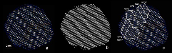
Three atomic-resolution images of a copper-indium-sulfur nanoparticle: (a) Only the copper and indium atoms are shown in blue and yellow; (b) Copper and indium atoms shown in same color demonstrating that they form a perfect hexagonal lattice; (c) Same as (a) with the boundaries between regions of distinct copper-indium order outlined. (Source: Vanderbilt)
 |
|
 |
|
 |
 |
 | |
 |
 |
Leave a Reply