Using tightly coupled droop detectors and adaptive clocking to reduce the impact of voltage droop due to workload variations.

Voltage droop, also known as IR drop, is a phenomenon that occurs when the current in the power delivery network abruptly changes due to workload fluctuations. This can lead to supply voltage drops across system-on-chips (SoCs) which can cause severe performance degradation, limit their energy efficiency, and in extreme cases can cause catastrophic timing failures. To avoid these issues, conventional designs apply clock frequency, voltage guard-bands, and/or software guard-bands which add power, architectural complexity, or cap performance. And in some cases the system designer may even be forced to contend with managing the workload in software, which adds complexity and other performance limitations.
In more bespoke solutions, teams are employing tightly coupled adaptive circuits that adjust dynamically in order to mitigate droop effects. However, these techniques have limitations such as response time and analog complexity, which has led some researchers to investigate all-digital resilient droop response solutions. In this blog post, we will explore the advantages of integrated or tightly coupled droop detectors and adaptive clocking for silicon circuits.
Conventional techniques for dealing with droop involve using clock frequency, voltage, and software guard-bands. In context, a frequency guard-band is a technique where a designer will intentionally reduce the maximum frequency to make sure that there are no timing glitches when a voltage droop occurs. A voltage guard-band is similar, except the designer will increase the minimum voltage (Vmin). The former ends up reducing overall system performance, while the latter increases average system power in an exponential manner (V2 relationship). Alternatively, design teams can implement software guard-bands to stagger loads and prevent an instantaneous rush of switching activity. However, it comes with its own performance penalty and can add architectural complexity in the software, firmware, and hardware stack.
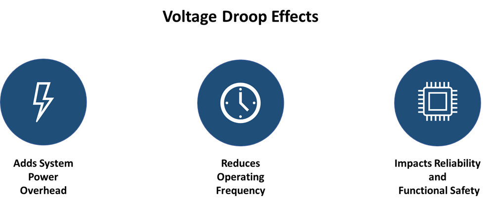
Fig. 1: Negative effects of static guard-banding and voltage droop.
The next step past static guard-banding, for voltage droop, is adaptive circuits. Adaptive circuits are designed to adjust to prevent critical path timing margin failure due to voltage droop. They typically involve a complex analog control loop which monitors the power supply voltage and current and adjusts the clock frequency in response. This is done by either adjusting the pull-up/pull-down transistors or by modulating the duty cycle of an oscillator. The goal of these adaptive circuits is to minimize any performance degradation caused by voltage droops while maintaining energy efficiency. To achieve this, they employ various techniques such as self-adaptive clocking, dynamic supply scaling, or adaptive voltage scaling depending on the application requirements. By making use of these adaptive techniques, they can provide higher levels of resilience against voltage droop events and allow for improved system performance and energy efficiency.
The limitations of these techniques in terms of response time and analog complexity are significant. The analog control loop used by adaptive circuits is complex and can be difficult to design and characterize. In addition, the adaptive techniques used may not be able to react quickly enough to sudden voltage drops as they suffer from high latency due to the slow speed of the analog circuitry and its dependence on external factors such as temperature. This limits their effectiveness at mitigating fast voltage droop events.
In recent years, researchers have explored the use of all-digital resilient timing error detection and recovery circuits as a way to mitigate voltage droops. These techniques make use of digital circuitry to detect and respond to voltage droop events in real time with minimal latency and can provide improved accuracy for detecting fast droop events compared to analog-based techniques. Furthermore, because they do not rely on complex analog components, they are able to scale efficiently with process nodes while still providing high levels of resilience against voltage droops. This makes them an attractive solution for reducing the impact of workload variations on system performance and energy efficiency.
Integrated or tightly coupled droop detectors and adaptive clocking provide numerous advantages for silicon circuits. These solutions leverage tightly coupled IP that pairs detection with an adaptive clock generator. The integrated system allows droop response to be fully self-contained within the system IP, allowing for impressively fast total time to adapt (detection + adaptation time). Across various papers, researchers found that tightly coupled droop response can reduce system power by more than 10% across various architectures (systolic arrays, manycore CPU arrays, and GPUs) (at 10% droop), relative to static guard-banding and minimize total time to adapt by more than 10x.

Table 1: Margin reclaimed from published tightly coupled droop response systems.
Integrated or tightly coupled droop detectors and adaptive clocking are a promising solution for reducing the impact of voltage droop due to workload variations, which primarily reduces system performance and energy efficiency. They leverage digital architectures for real time detection with minimal latency, allowing them to react quickly to sudden drops in supply voltage. Additionally, they less complex and more process portable than analog-based solutions as they do not require complex control loops or vary with external factors such as temperature. Integrated or tightly coupled droop response solutions deliver significant system power savings while creating a self-contained, swift droop response solution.
References
[1] S. K. Lee, P. N. Whatmough, N. Mulholland, P. Hansen, D. Brooks, and G.-Y. Wei, “A wide dynamic range sparse FC-DNN processor with multi-cycle banked SRAM read and adaptive clocking in 16 nm FinFET,” in Proc. IEEE 44th Eur. Solid State Circuits Conf. (ESSCIRC), Sep. 2018, pp. 158–161
[2] M. S. Floyd et al., “26.5 Adaptive clocking in the POWER9 processor for voltage droop protection,” in IEEE Int. Solid-State Circuits Conf. (ISSCC) Dig. Tech. Papers, San Francisco, CA, USA, Feb. 2017, pp. 444-445
[3] K. Wilcox et al., “Steamroller module and adaptive clocking system in 28 nm CMOS,” IEEE J. Solid-State Circuits, vol. 50, no. 1, pp. 24–34, Jan. 2015
[4] T. Hashimoto et al., “An adaptive-clocking-control circuit with 7.5% frequency gain for SPARC processors,” IEEE J. Solid-State Circuits, vol. 53, no. 4, pp. 1028–1037, Apr. 2018
 |
|
 |
 |
 |
 |
Leave a Reply