Using embedded FPGAs in low-power applications.

Datacenters heavily leverage FPGAs for AI acceleration. Why not do the same for low power edge applications with embedded FPGA (eFPGA)?

It’s common knowledge for anyone connected to the cloud computing industry that data centers heavily rely on FPGAs for programmable accelerators enabling high performance computing for AI training and inferencing. These heterogeneous computing solutions evolved due to diminishing performance returns with shrinking processes nodes. Similar heterogeneous performance gains can also be had with ASICs, ASSPs (applications specific standard parts) and MCUs with eFPGA.
Chip designers for edge IoT, consumer, mobile and communications devices are always pushing for the highest performance at the lowest power. Power limitations constraining performance in SoCs occur for many reasons such as process (e.g. huge investment prohibits moving to smaller geometries), software investment around a processor architecture or implementation make it difficult to either upgrade to a higher performance processor (if there is one) or adding more parallel processors, or the processor may simply not be the best compute engine to execute complex workloads like inferencing, parallel processing, filtering, and compression that require a lot of clock cycles (and consume lots of power) to execute that function.
With these types of constraints, designers can borrow a data center architect’s playbook by integrating eFPGA in their ASIC. After all, if you stretch your imagination a bit, an SoC is a tiny data center. Most SoCs today are not leveraging the power of FPGA based programmable accelerators which means there’s a wealth of opportunity to greatly increase performance in SOCs without having to radically change a chip’s manufacturing process or hardware or software architecture.
eFPGA for AI acceleration, as an example, can be the solution for a wide spectrum of requirements. For CPU centric solutions, a processor’s instruction set can be augmented with instructions tuned for a particular inferencing model. For higher performance and a more traditional approach, a larger eFPGA fabric can be integrated to execute complex inferencing engines developed and used in FPGAs. In the latter case, even though the SOC power may increase, the overall system solution power will decrease because a set of power-hungry SerDes are removed when the FPGA chip is removed, not to mention cost and board space.
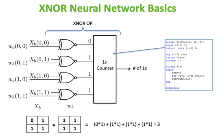
For applications that do not need a high degree of accuracy, a more generic solution maybe more suitable by attaching a small amount of eFPGA to the system bus and programming it with an XNOR or bi-neural network which uses a minimal number of LUTs.

You can see a demo of an XNOR model recognizing characters with only 200 LUTs here. When not used for AI acceleration, it can be programmed with other non-AI centric workload accelerators or powered off to save power.
With the availability of silicon proven eFPGA availability in many different popular process nodes, designers can now put data center processing power in their SoCs for edge applications and solve heterogenous computing and AI acceleration whether big or small. Now you, too, can put a datacenter in your phone!
Leave a Reply