A LAB process where the laser emission from the bottom BGA side to bump is transmitted through the stage vacuum block.

By SeokHo Na, MinHo Gim, GaHyeon Kim, DongSu Ryu, DongJoo Park, and JinYoung Kim
In the recent semiconductor market, there are many applications including smartphone, tablets, central processing units (CPUs), artificial intelligence (AI), data cloud and more that are expecting and experiencing rapid growth. As most of these applications require high performance, single-die Flip Chip packages may no longer be appropriate and multi-dies in a chiplet module packages could be the new solution. From the viewpoint of the bump interconnection methodology, mass reflow (MR), thermocompression bond (TCB) and laser assisted bonding (LAB) are widely used in the industry. For LAB, the technology and bonding mechanism have been reported with a general comparison of bonding methods shown in table 1 [2].
The focus of this study is on LAB technology for chiplet module bonding on substrate. Reverse laser assisted bonding (R-LAB) technology is introduced to overcome the limitations of the existing top LAB. R-LAB results are compared with top LAB. Test units were built with an optimized R-LAB recipe, submitted to reliability testing and checked with Open/Short (O/S) testing, scanning acoustic tomography (SAT) inspection and bump interconnection quality for any abnormality post reliability.

Table 1: Comparison of flip chip bonding methods.
The test vehicle is a Substrate SWIFT (S-SWIFT) package. The package body size is 2500 mm2, and the module size is 650 mm2 with 770 µm thickness. Bump pitch is a minimum of 110 µm with a 60 µm circular bump diameter. The total bump height is 60 µm by 40 µm for the copper (Cu) pillar bump with a 20 µm tin-silver (SnAg) solder cap. The organic substrate has 10 Cu layers, a Solder on Pad (SOP) finish and the total thickness is 1.66 mm. The package schematic image is shown in figure 1. Additional information for the test vehicle is summarized in table 2.

Fig. 1: Schematic image of S-SWIFT packaging.

Table 2: Description of test vehicles.
Prior to evaluating the R-LAB units, the existing top LAB evaluation was performed. Bump interconnection performance was checked based on infrared (IR) peak temperatures by changing laser conditions. All legs showed EMC burn out and resulted in bump non wet. The EMC burn out may have occurred due to low heat transmittance of EMC (EMC 0.9W/mK vs. Si wafer 14.9W/mK). Due to the lack of heat, the bump underneath the EMC could not make a bump interconnection. Furthermore, the EMC burning is more severe as peak temperatures increased. Leg 4 with the highest peak temperature only shows partial wetting while other legs show complete die separation. Summary results are described in table 3.
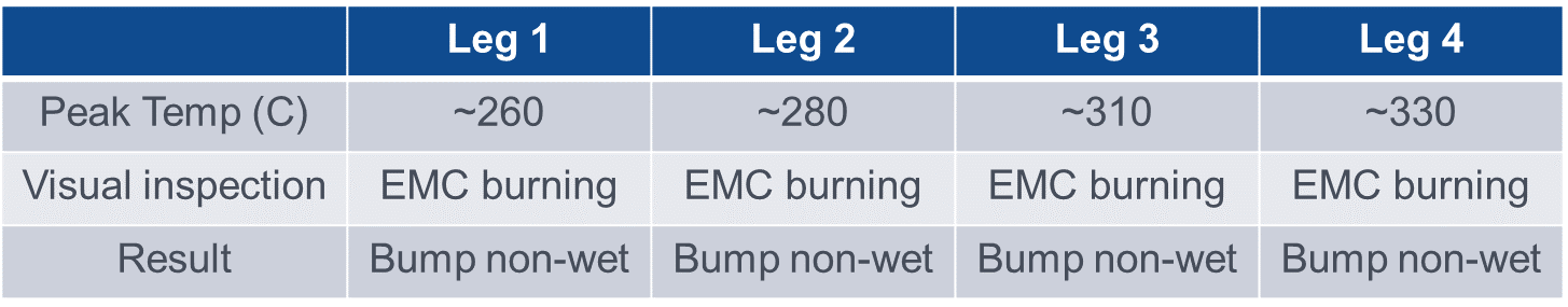
Table 3: Top LAB evaluation result.
The visual inspection image of the module’s side view, top view and bump cross section image are shown in Figure 2.

Fig. 2: Visual inspection and X-ray images of each leg with existing top LAB process.
Based on these results, it is very hard to find optimum LAB conditions using a top LAB design.
To avoid the EMC burning with top LAB, a reverse type of LAB using laser emission from the bottom ball grid array (BGA) side to bump by transmission through stage block was proposed. This R-LAB should overcome the limitations of existing top LAB. Target applications would be backside metallization (BSM) die, DRAM in an epoxy molding compound (EMC) package and chiplet module interconnections on substrate. Figure 3 shows schematic images of the existing top LAB and the R-LAB in detail.

Fig. 3: Schematic image of existing top LAB (top) and R-LAB (bottom).
After a couple of trials adjusting power and time, optimum R-LAB conditions were achieved. Figure 4 shows the results of good bump interconnections without any bump non-wet, bump short or substrate surface damage at the BGA side or EMC burning.

Fig. 4: Visual inspection images (top) and bump cross-section images (bottom).
Next, measurements were made of the peak temperature of the chiplet module. An IR camera was used to measure the temperature of silicon back side. The temperature of the bump area was measured by a thermocouple (TC). The thermocouple was inserted between the die and substrate at both die corner and die center positions as shown in figure 6. The IR peak temperature of the chiplet module is around 240~250°C and substrate surface temperature is around 250~260°C from the optimized recipe. The thermocouple temperature at the bump is around 260~266°C which exceeds the solder melting temperature. The IR peak image, IR temperature profiles and thermocouple profiles are shown in figure 5 and figure 6 respectively.

Fig. 5: IR peak image (left) and IR profiles (right).

Fig. 6: X-ray images of TC kit (left) and temperature profile (right).
In addition to the chiplet module bonding on substrate, BSM die application and DRAM attach will need reverse LAB technology. Development continues for both applications and, to date, has achieved promising results with good interconnections. Promising BSM die evaluation results are published in recent 72nd ECTC [1]. Table 4 shows the schematic image of the R-LAB applications.

Table 4: Schematic images of R-LAB applications.
Test units were built with an R-LAB optimized recipe and subjected to reliability tests. At each reading, Open/Short (O/S) tests and SAT inspection were performed. Additionally, bump cross section was done to see if there were any post-reliability abnormalities. As a result, all reading points showed no O/S failures, no SAT abnormalities, and no abnormalities appeared in bump cross section. Tests include moisture sensitivity testing level 4 (MSL4), Unbiased Highly Accelerated Stress Test (UHAST) of 264 hrs., Temperature Cycle, Condition B (TCB) 1000X and high temperature storage (HTS) of 1000 hrs. as shown as shown in Table 5 and Figure 7 respectively.

Table 5: Reliability test results.

Fig. 7: Typical bump cross-section images post each reliability testing.
This study demonstrated the viability of bump interconnection of chiplet module on substrate using LAB technology. Due to the low heat transmittance of EMC, normal top LAB conditions are not feasible due to lack of heat transfer to the bump that resulted in non-wet regardless of laser power conditions. The conclusion was that it is very hard to optimize the LAB conditions and the process margin would be very narrow. Existing top LAB is not recommended for chiplet module interconnections on substrate.
To improve quality, reverse LAB was developed. This is a reverse-type LAB where the laser emission from the bottom BGA side to bump is transmitted through the stage vacuum block. The R-LAB process shows promising results without observing substrate BGA side surface damage, EMC burning, bump non-wetting or bump shorts for the 110-µm bump pitch of the module test vehicles. Parts built with an optimized LAB condition show no abnormalities at O/S test and SAT and the bump interconnections passed all reliability tests through MSL4, UHAST 264 hrs., HTS 1000 hrs., TCB 1000X. R-LAB was developed to overcome the limitation of existing LAB and it may provide a better solution for the fine pitch of chiplet module bonding on substrate. This will also be a potential solution for BSM die interconnections and DRAM in an EMC bonding as well.
This study was supported by the Amkor Technology Global R&D center. The authors would like to give special thanks to the R&D Center, LAB team, FA team and reliability test team members.
SeokHo Na, MinHo Gim, GaHyeon Kim, DongSu Ryu, DongJoo Park, and JinYoung Kim are part of the Advanced Process & Material Development, Global R&D Center at Amkor Technology Korea.
 |
|
 |
|
 |
 |
 | |
 |
 |
Leave a Reply