Data output processed by EDA design and analysis tools must become standardized at the API level.

By Rajeev Jain, Kerim Kalafala, and Ramond Rodriguez
Significant technology disruptions are on the horizon that will provide massive efficiency gains for EDA tool suppliers and semiconductor companies alike. These disruptions include the application of artificial intelligence and machine learning to enhance supplier tools and optimize user design flows and methodologies, and the ensuing migration of EDA tools to the cloud. With the advent of increasingly sophisticated analysis capabilities (e.g., the use of statistical static timing analysis to cover an exponential number of process corners for sign off), the volume and velocity of processed data generated during the life cycle of IC design implementation are far outstripping the ability of our existing systems to enable efficient collaboration in AI/ML and the migration of EDA tools to the cloud.
Looking ahead to the need for more efficient implementation of design flows and co-optimization of design technologies, the data output processed by EDA design and analysis tools must become standardized at the API level—just as design data input has been standardized. This will create significant interoperability and cost efficiencies comparable to the standard, OpenAccess API and reference code contributed to Silicon Integration Initiative (Si2) by Cadence. Where feasible, augmenting and replacing the person-in-the-loop design and analysis with intelligent automated systems will preserve and extend our aging design community’s collective knowledge and expedite development of faster learning and intelligent solutions. Lack of interoperability threatens the realization of this vision, however, and the entire industry would suffer if the gains in efficiency promised by AI and ML were overshadowed by the integration costs, lack of interoperability, and time wasted in file and format translations between processed EDA tool data and AI engines.
Standardized access to processed data is critical to head off such a wave of new inefficiencies and would be best achieved through a new, open, and secure API. For future-safe operation, this API should be cloud-aware, enabling communication between cloud applications as well as between cloud and user-hosted applications. The API must also have sufficient intelligence to provide secure, real-time translation, and secure, customizable access to data deemed proprietary. This requires that, depending on the requesting actor’s identity and intended use, proprietary data be automatically protected by obfuscation, normalization, and quantization, from inception through storage and eventual use.
To further support this innovation, the OpenAccess database should be extended for use in cloud environments by developing RESTful API extensions. This would enable OpenAccess-based applications to directly serve out select design data to other applications, including ML feature stores.
An early-stage vision of a near-future hybrid cloud infrastructure, which encapsulates features of both cloud and user-hosted tools, is shown in figure 1. In this environment, EDA tools and higher-level engines can request data from other tools, engines, and OpenAccess and processed data databases. Cloud-based tools relying on common design data and serving out standard-format processed data would employ both an OpenAccess API and the secure, processed data API for data exchange.

Fig. 1: Near-future hybrid cloud infrastructure vision.
A near-term, substantial productivity improvement can be realized by providing simply one enabling piece of the envisioned infrastructure. As implementation (training and inference) of AI and ML for current and future environments will require access to significant amounts of structured and properly labeled datasets, efficiency gains will be realized if this data is available via EDA tools providing processed (output) data, through a secure, standard API, into a processed-data database. Figure 2 illustrates this concept.
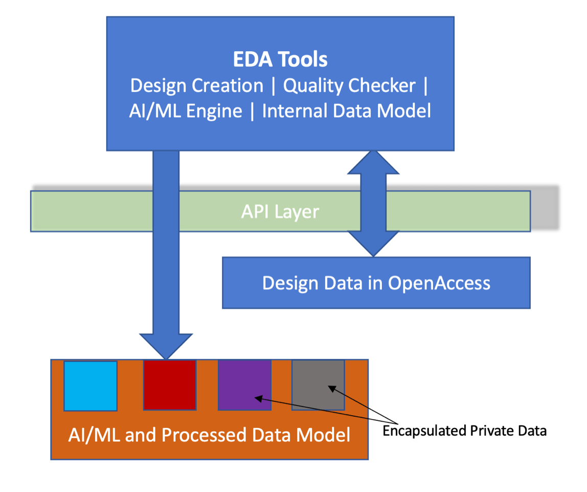
Fig. 2: Secure processed data API.
The industry is developing AI methods to tackle the inability of existing heuristics to scale with exponentially increasing PVT corners and design complexity. The lack of open APIs for EDA processed data is already hampering deployment of these methods, resulting in sub-optimal designs and higher-cost products to the consumer. These impacts will only broaden as AI/ML permeates semiconductor design flows, suggesting that a lack of open APIs may be a chief obstacle to widespread deployment of AI methods. Forming a secure, processed data API working group at Si2 is the first step toward a collaborative solution.
Rajeev Jain is a senior director of technology at Qualcomm.
Kerim Kalafala is a senior technical staff member at IBM.
Ramond Rodriguez is a senior director of strategic CAD capabilities at Intel.
 |
|
 |
 |
 |
 |
Leave a Reply