Completely separating the power delivery network from signal wiring provides a range of benefits, from IR drop reduction to chip area scaling.

One part of the short course that I attended at IEDM in December was about backside power delivery networks. It was presented by Gaspard Hiblot of imec and titled “Process Architectures Changes to Improve Power Delivery.” The presentation is co-credited with Geert Hellings and Julien Ryckaert. I should preface this post with the fact that this presentation was 80 slides long and so I will only be covering some of the most important aspects of what was presented.

Modern process design goes hand in hand with designing some aspects of the silicon structures that will be used. This is very different from how it was done a decade ago when the process technology development team would basically give the design groups a set of SPICE models and a set of layout design rules. This new approach goes under the name Design Technology Co-Optimization, or DTCO. I first came across this in 2016 at CDNLive Europe, where Luca Matti presented the work he was doing at imec on the then up-and-coming process nodes of 7nm and 5nm. I covered his presentation in my post CDNLive: Design Technology Co-Optimization for N7 and N5. In the early days of DTCO, the focus was on adding tweaks to the semiconductor process, such as contact-over-active-gate, that would enable standard cells to be built with fewer tracks. You can see some of the DTCO tradeoffs in the 2018 era in my post, Imec Roadmap which Diederik Verkest presented to me when I visited imec that year.
As I’m sure you have heard, simple dimensional scaling (aka Moore’s Law) is running out of steam, and DTCO approaches are required to keep scaling on track. One big challenge is via resistance. Historically, vias have been manufactured using copper since it has low resistance. But copper needs a diffusion barrier, such as TaN, which has two issues. Firstly, it reduces the cross-sectional area of the copper in the via since the barrier takes up some space. Secondly, the barrier exists at the bottom of the via, and the current has to flow through it. Since barrier metals are higher resistance than copper, this results in a higher resistance via.
Copper lines have similar problems, and the resistivity of the copper itself starts to increase below 100nm line width due to both grain size in the copper and the increasing percentage of the space that is taken up by the sidewall. Ruthenium is often proposed as a solution to this since it doesn’t require a barrier and has better resistivity at the smallest dimensions. But, as far as I know, nobody has switched from copper to ruthenium. There is some use of cobalt in the lowest level vias, and perhaps even the M0 interconnect.

These issues with interconnect affect signals, clocks, and power. However, the tradeoffs for signal wiring and for the power delivery network (PDN) are different. Power wants low resistance and doesn’t care about capacitance much (because the voltage is not changing). But it needs to convey large currents, making electromigration a big concern, which it is not for normal signals. The solution is to differentiate power and signal wiring at the cost of a more complex process.

But the ultimate differentiation is to separate the PDN from the signals completely and create a backside PDN. This is just what it sounds like. The PDN is built on the back of the thinned wafer and connected to the transistors and frontside interconnect using through silicon vias (TSVs).
Backside power delivery networks (BS-PDN) have several value propositions:
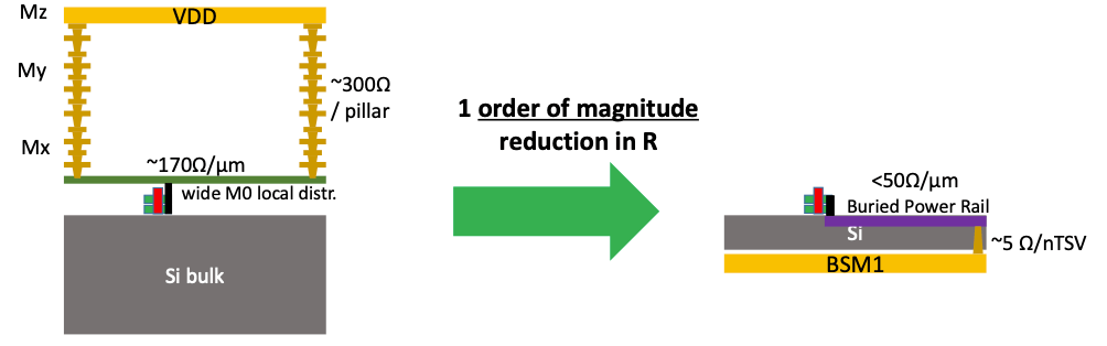
First, BS-PDN reduces on-chip IR drop by an order of magnitude, as you can see in the above diagram, where a via pillar of about 300Ω is reduced to a TSV of just 5Ω. This also significantly reduces on-chip IR drop.
Second, BS-PDN scales chip area. This depends critically on various aspects of the process (such as the size of the keep-out zones around TSVs) and also on the EDA tools. The router in a tool like Innovus “should” have an easier time routing signals without the PDN creating blockages in the interconnect stacks. But just how big a gain is obtained requires experiments.

The buried power rail (BPR), if used, gives about 15-20% scaling too since the number of tracks in the standard cells can be reduced.
The third benefit of backside power is that it reduces the complexity of the fine metal in the BEOL. It is not easy to mix wide (for power) and narrow (for signal) on the same layers with the usual dual damascene approach used for copper.

Fourth, backside power makes it easier to do wafer-on-wafer bonding to stack memory on logic. The flipped SRAM die is powered from the logic die, so effectively by the same BS-PDN.

There are three basic approaches to BS-PDN (see the above diagram):
In the presentation, Gaspard went through each of these in some detail. I’m going to focus on the issues that are common to all three approaches, what he called “common challenges.” The details of the three flows dive deep into process technology flows, which is beyond the scope of this blog.

The first challenge is that backside power requires extreme thinning of the silicon wafer to less than 10µm. A second wafer has to be bonded to the real wafer (for mechanical support and manipulation) before the real wafer is ground down (as in the picture above).
In all the approaches, another challenge is aligning the backside to the frontside. The nano-TSVs (nTSVs) need to be aligned within about 10nm.

Above is the high-level flow for TSV-middle.

And now for BPR (buried power rail).

There seem to be two candidates for the material for the BPR, tungsten (W) and Ruthenium (Ru). Tungsten has a lower contamination risk and meets the target resistance of 50Ω/µm. But barrierless ruthenium has a lower via resistance.
I won’t say much about the backside contact approach since it seems to be a long way off from being practical. Gaspard’s summary was:
The last section of the presentation was on possible future developments.

One thing that springs to mind almost the moment you hear about backside power is whether we can go further and create a functional backside and then migrate some system functions to the backside. First is global interconnect (not requiring devices on the backside). But there is the possibility of backside devices too.

Another obvious thing to try and do on the backside is to create metal-insulator-metal capacitors (MIMCAP). MIMCAP can help to reduce dynamic IR drop given the large power densities that can be involved (1W/mm2).

It is clear that backside power will continue to evolve, complementing the logic device roadmap.
 |
|
 |
 |
 |  |
 |  |
Leave a Reply