Alternatives to CD-SEM with higher throughput, better layer transparency, and the ability to add additional parameters.

By Honggoo Lee, Sangjun Han, Minhyung Hong, Seungyong Kima, Jieun Lee, DongYoung Leea, Eungryong Oh, and Ahlin Choi of SK Hynix, and Hyowon Park, Waley Liang, DongSub Choi, Nakyoon Kim, Jeongpyo Lee, Stilian Pandev, Sanghuck Jeon, John C. Robinson of KLA-Tencor
Abstract
Overlay is one of the most critical process control steps of semiconductor manufacturing technology. A typical advanced scheme includes an overlay feedback loop based on after litho optical imaging overlay metrology on scribe-line targets. The after litho control loop typically involves high frequency sampling: every lot or nearly every lot. An after etch overlay metrology step is often included, at a lower sampling frequency, in order to characterize and compensate for bias. The after etch metrology step often involves CD-SEM metrology, in this case in-cell and on-device. This work explores an alternative approach using spectroscopic ellipsometry (SE) metrology and a machine learning analysis technique. Advanced 1x nm DRAM wafers were prepared, including both nominal (POR) wafers with mean overlay offsets, as well as DOE wafers with intentional across wafer overlay modulation. After litho metrology was measured using optical imaging metrology, as well as after etch metrology using both SE and CD-SEM for comparison. We investigate two types of machine learning techniques with SE data: model-less and model-based, showing excellent performance for after etch in-cell on-device overlay metrology.
1. Introduction
Overlay process control has been a critical part of integrated circuit manufacturing for many years. As design rules shrink, the requirements for overlay control become more challenging. A typical scheme includes an overlay feedback loop based on after litho overlay metrology, also known as ADI (after develop inspection). The ADI overlay control loop is typically based on optical metrology of scribeline targets, either image-based metrology or scatterometry-based. Typical sampling at ADI is high frequency, either every lot or every few lots. Yield is linked to after etch overlay, in-cell, on device, and at design rule. To bridge this gap, after etch metrology or AEI (after etch inspection) is added to characterize and correct for the bias. AEI overlay metrology is often done with a CD-SEM in order to measure in-cell, on-device, and at design rule. Typically, AEI metrology for bias compensation is done on a lower frequency, such as every few weeks. There is an industry push to increase the frequency of AEI overlay metrology, invoking the use of high-throughput SEM defect review tools for example. This study offers an alternative to the use of a SEM. The overlay control scheme used for advanced 1x nm DRAM is depicted schematically in Figure 1 [1, 2]. Analysis tools, such as 5D Analyzer, are used to combine the ADI and AEI results into modeled correctables suitable for process control.
CD-SEM based overlay metrology for AEI bias compensation, however, has shortcomings. CD-SEM tools have relatively low throughput (or conversely high cost-of-ownership), have limited layer transparency, poor precision compared to optical methods, are often destructive to the measured pattern, and provide very little profile information. Spectroscopic ellipsometry (SE), however, has the potential to overcome all of these obstacles. SE has been in use for many years for CD metrology [3] and has also demonstrated the ability to measure overlay in-cell, on-device, and at design-rule. Additionally, it has relatively high throughput, high precision, and can provide full profile information. Being optical it has good layer transparency in many cases, which is critical for buried layer metrology, and it is generally non-destructive to the measured pattern.

Figure 1: Overlay process control schematic including after develop inspection (ADI) and after etch inspection (AEI) overlay metrology with feedback to the litho cell.
In this work we take advantage of a key innovation in spectroscopic ellipsometry analysis. Called TurboShape®, it uses an advanced machine learning technique [4, 5] rather than the conventional full rigorous model-based approach. TurboShape, as it is called here, requires a training set of data. The training set includes an intentionally overlay-modulated wafer with programmed values. Spectra from the training set are kept as a reference and then compared with spectra from wafers under test. TurboShape can be done both with and without models, has much quicker setup time, and potentially many more degrees of freedom than conventional rigorous model based approaches. TurboShape is depicted schematically in Figure 2.

Figure 2: TurboShape workflow overview.
2. Recipe development and wafer preparation
For this study, the starting point is the development of the 1x nm DRAM wafers. Two types of wafers were created; 3 DOE (design of experiment) and three off-set POR (plan of record, or nominal) wafers. To make the DOE wafers, 5D Analyzer was used to create a scanner sub-recipe to provide intentional across wafer overlay modulations of known amounts. Additionally, three wafers with constant nominal overlay, but with fixed mean offsets (-5 nm, 0 nm, and +5 nm), were created (here called POR waters). All six wafers were measured with an SE, and with a CD-SEM for comparison as shown in Figure 3. The three DOE wafers were used for recipe setup. The three POR wafers were not part of the recipe training set.
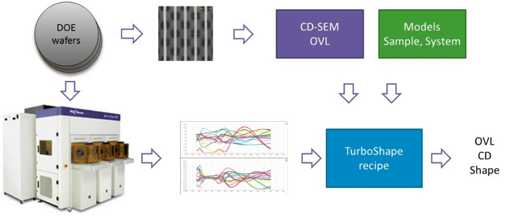
Figure 3: TurboShape recipe development. DOE wafers are used for TurboShape recipe generation and CD-SEM comparison.
As shown in Figure 4, both sets of wafers, the DOE and the POR, were measured at ADI on the Archer™ 600 optical imaging system on scribe-line metrology marks. After etch processing, both sets were measured on an SE and CD-SEM. In the AEI case, measurements were done in-cell, on-device, and at design-rule at the same locations on SE and the CD-SEM for paired population comparisons. All fields are measured, and there are seven measurement sites per field.

Figure 4. Both DOE and off-set POR were measured at ADI and AEI. Metrology was done on all fields and seven sites per field.

Figure 5. Comparison of overlay variability by wafer for (a) ADI optical imaging, and (b) AEI CD-SEM. Small variability for off-set POR wafers, and large variability for DOE wafers.
In Figure 5 we compare variability across the set of six wafers. Wafers 4, 5, and 6 are the DOE modulated wafers used for recipe training. Whereas the mean value is close to zero, the variability is large as expected. Wafers 1, 2, and 3 are the POR off-set wafers. In this case the variability is relatively less, but the means differ as expected. Shown here are ADI results based on optical imaging metrology as well as AEI CD-SEM results. Figure 6 shows the same results as wafer map signatures. Both the ADI optical imaging results and the AEI CD-SEM results are qualitatively similar. The three off-set POR wafers are fairly constant, though at different values, and the DOE wafers show the intentional overlay modulation.

Figure 6. Wafer map overlay signatures for ADI imaging and AEI CD-SEM, for both off-set POR wafers and DOE wafers.
3. Model-less overlay results
TurboShape uses an advanced machine learning algorithm to extract relevant information from SE spectra to estimate the target of interest. Compared to other techniques that attempt to measure overlay as an asymmetry and are affected by symmetric and asymmetric process variations, TurboShape recipe is trained to measure actual overlay and it is robust to the effects of other asymmetries and process variations.
TurboShape can perform in two modes: model-less and model-based. In the model-less case, spectra from the DOE are measured and used as explanatory variables to the TurboShape machine learning algorithm. CD-SEM overlay serves as a reference to supervise model calibration (training the algorithm). In the process of training the TurboShape recipe becomes insensitive to process variations that are occurring naturally within the DOE wafers. The resulting TurboShape recipe is robust to process variation and captures the relationship between spectra and reference, which can be deployed to accurately estimate overlay given new spectra. A sketch of this procedure is shown in Figure 7. Unlike conventional rigorous model based SE methods, no stack or prior layer information is required, and setup time can be extremely quick.

Figure 7. TurboShape model-less recipe development workflow.

Figure 8: TurboShape AEI overlay measurements (left) and correlation to CD-SEM AEI overlay. SRM denotes TurboShape.
Figure 8 shows AEI overlay results from the model-less analysis. The variability shown at left are comparable to the results shown in the previous section. Also, there is good correlation between the CD-SEM results and the TurboShape results, with r-squared of 0.98 and slope of 0.99. Figure 9 shows the POR wafers, which were not used to train the recipe. Again we see nominally flat wafers with fixed mean offsets. The correlation of wafer mean between SE and CD-SEM are excellent with r-squared of 0.99 and slope of 1.0.

Figure 9: Model-less off-set POR AEI overlay wafers (left) and correlation to CD-SEM overlay (right). SRM denotes TurboShape.
4. Model-Based Overlay, CT, And Profile Results
As an alternative option, TurboShape analysis of SE spectra can perform in the model-based mode. In this case the DOE wafers are used without requiring CD-SEM calibration results, as shown in Figure 10. The needed spectra and the reference values of the DOE in this case are generated from the models, providing full control over the ranges of variations and the number of floated parameters. The TurboShape recipe created by this method is robust to process variations over large parameter ranges and allows for effectively floating many more parameters (compared to traditional optical critical dimension [OCD]). This makes the TurboShape measurements accurate and not affected by the “Fixed Parameter Errors” (FPE) – errors typical for the traditional OCD. This method has the added advantage that in addition to overlay, other parameters can also be estimated including CD, and shape or profile. Again, the setup time of this method is significantly shorter than that of the traditional rigorous model-based approach.

Figure 10: TurboShape model-based recipe development workflow.
In this model-based case, we see similar AEI results to those shown previously. The DOE wafers show large programmed variation, and the POR wafers show minimal variation but fixed offsets, all as expected. The comparison of model-based to CD-SEM, again, shows good correlation, with an r-squared of 0.96 and a slope of 0.92, as shown in Figure 11. A slight saturation can be seen at the low end which requires further investigation. In Figure 12, we see the comparison of the POR wafers, which were not used for the recipe calibration, between model-based SE and CD-SEM. The correlation is again excellent, with r-squared of 0.99 and slope of 0.93.

Figure 11: Model-based TurboShape AEI overlay variability by wafer (left), and correlation of TurboShape overlay with CD-SEM AEI overlay (right).

Figure 12: Model-based off-set POR AEI overlay wafers (left) and correlation to CD-SEM overlay (right). SRM denotes TurboShape
One advantage of the model-based approach is that simultaneous additional parameters beyond overlay can be determined, including profile and CD values. Figure 13 plots four critical parameters as a function of radius, showing consistent and expected radial wafer map signatures. Additional parameters can be used in process control to isolate process changes such as CMP, etch asymmetries, etc.

Figure 13: Critical profile (CP) parameter measurements as a function of wafer radius for six wafers.
5. Summary and conclusions

Figure 14: Summary comparison for TurboShape model-less and model-based AEI overlay results vs. CD-SEM AEI overlay results: r-squared, slope, and intercept.
Overlay process control schemes in 1x nm DRAM include a high frequency ADI feedback loop, typically based on optical targets located in the scribe line. Lower frequency AEI sampling is used for periodic bias corrections, based on in-cell, on-device, at design-rule CD-SEM measurements. CD-SEMs have several drawbacks which were discussed above. In this work we demonstrate SE and TurboShape as an alternative to the CD-SEM with comparable performance (Figure 14), higher throughput, better layer transparency, and the ability to provide additional parameters. TurboShape has advantages over conventional rigorous model-based SE analysis including faster time to recipe setup. ADI and AEI feedback are combined and modeled for advanced process control and improved yields, as discussed previously, for example with 5D Analyzer [1, 2].
6. References
[1] Honggoo Lee, Sangjun Han, Jaeson Woo, DongYoung Lee, ChangRock Song, Hoyoung Heo, Irina Brinster, DongSub Choi, John C. Robinson, “High-volume manufacturing device overlay process control,” Proc. SPIE 10145, Metrology, Inspection, and Process Control for Microlithography XXXI, 101450D (28 March 2017).
[2] Honggoo Lee, Sangjun Han, Youngsik Kim, Myoungsoo Kim, Hoyoung Heo, Sanghuck Jeon, DongSub Choi, Jeremy Nabeth, Irina Brinster, Bill Pierson, John C. Robinson, “Device overlay method for high volume manufacturing,” Proc. SPIE 9778, Metrology, Inspection, and Process Control for Microlithography XXX, 97781F (18 March 2016).
[3] John A. Allgair, David C. Benoit, Robert R. Hershey, Lloyd C. Litt, Ibrahim S. Abdulhalim, William Braymer, Michael Faeyrman, John C. Robinson, Umar K. Whitney, Yiping Xu, Piotr Zalicki, Joel L. Seligson, “Manufacturing considerations for implementation of scatterometry for process monitoring”, Proc. SPIE 3998, Metrology, Inspection, and Process Control for Microlithography XIV, (2 June 2000).
[4] Stilian Pandev, Fang Fang, Young Ki Kim, Jamie Tsai, Alok Vaid, Lokesh Subramany, Dimitry Sanko, Vidya Ramanathan, Ren Zhou, Kartik Venkataraman, Ronny Haupt, “Signal response metrology (SRM): a new approach for lithography metrology,” Proc. SPIE 9424, Metrology, Inspection, and Process Control for Microlithography XXIX, 94241P (19 March 2015).
[5] Fang Fang, Xiaoxiao Zhang, Alok Vaid, Stilian Pandev, Dimitry Sanko, Vidya Ramanathan, Kartik Venkataraman, Ronny Haupt, “Improving OCD time to solution using Signal Response Metrology,” Proc. SPIE 9778, Metrology, Inspection, and Process Control for Microlithography XXX, 977806 (24 March 2016).
This was originally published in SPIE Advanced Lithography Conference 2018: Metrology, Inspection, and Process Control for Microlithography XXXII, edited by Vladimir A. Ukraintsev, Proc. of SPIE Vol. 10585, 105851D · © 2018 SPIE · CCC code: 0277-786X/18/$18 · doi: 10.1117/12.2300946
 |
|
 |
|
 |
 |
 | |
 |
 |
Leave a Reply