Understanding the benefits and challenges of a new, next-generation semiconductor architecture

In our November 2019 blog [1], we discussed using virtual fabrication (SEMulator3D) to benchmark different process integration options for Complementary-FET (CFET) fabrication. CFET is a CMOS architecture that was proposed by imec in 2018 [2]. This architecture contains p- and n-MOSFET structures built on top of each other, instead of having them located side-by-side. In our previous blog, we reviewed the use of different starting substrates (Si bulk, SOI, DSOI) and their specific challenges and opportunities with respect to CFET fabrication. We only considered Fin (or Nanowire)-based transistor structures in our prior study.
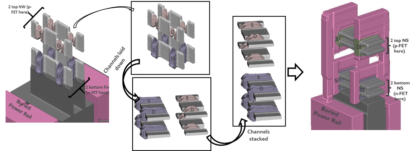
In collaboration with imec, we have now extended our earlier benchmark study to review a new design comprised of horizontal nanosheet transistors. This new CFET design is formed by using two stacks (one for n- and one for p-transistors) of two Nanosheets, processed one on top of the other. Figure 1 depicts the geometrical evolution from a Nanowire-On-Fin CFET to a Nanosheet-On-Nanosheet CFET design.

Fig 1: Geometrical CFET evolution from a 2 Nanowires-On- 2 Fins architecture to 2 Nanosheets-On- 2 Nanosheets architecture (NW: Nanowire, NS: Nanosheet, S: Source, D: Drain)
Benefits of New CFET Architecture
This new CFET architecture has two key benefits, highlighted in a recent paper published in the Journal of the Electron Devices Society [3]:
Modeling Process Challenges of Nanosheets in a CFET Design
The CFET Nanosheet-On-Nanosheet architecture presents one key technical challenge during Replacement Metal Gate (RMG) process integration. Specifically, during the metal recess step, metal must remain on the two bottom nanosheets while it is being completely removed both on and in-between the two top nanosheets. In order to assess the feasibility of this process, we used the SEMulator3D Process Window Optimization (PWO) module [4] to determine process and process window requirements. Five process parameters were considered in our PWO study:
One thousand (1,000) virtual wafer runs were executed with different distributions provided for each of the parameters. We used a nominal value, standard deviation and search space range for each parameter listed earlier. The PWO module calculated the process window required to ensure that the RMG integration flow was successful. The results (see Figure 2) indicated that:

Fig 2: Top – details on the distribution details for the five parameters considered in the 1000 run virtual DOE ; Bottom – SEMulator3D Process Window Optimization interface showing target and standard deviation values for each of the five parameters studied to reach a 99.8% predictive in-spec percentage target.
Conclusion
In conclusion, prior to Si wafer processing or tapeout, virtual processing allowed us to:
Virtual fabrication is a very attractive methodology for technology pathfinding development. It supports a greater number of technology and process experiments than is possible using wafer-based experimentation, with a much faster turnaround time and lower cost.
References
[1]https://www.coventor.com/blog/a-study-of-next-generation-cfet-process-integration-options/
[2] https://www.imec-int.com/en/articles/imec-presents-complementary-fet-cfet-as-scaling-contender-for-nodes-beyond-n3
[3] https://www.coventor.com/paper/benchmark-study-complementary-field-effect-transistor-cfet-process-integration-options-virtual-fabrication/
[4] https://www.coventor.com/blog/control-variability-semi-process-window-optimization/
Leave a Reply