Advancements in monitor analytics paving the way for automation of high-value applications.

When it comes to measuring key operational metrics such as power and performance of your silicon, in-chip monitors have been the longstanding cornerstone for providing such valuable measurements and insights. Data captured from these monitors – process monitors configured in the form of ring oscillator chains being the most common – can tell you if your chip is meeting the requisite power or performance requirements during the chip manufacturing stage prior to being put into the end device. However, the challenge today is that the analysis of this data, assuming you can collect all of it during manufacturing testing, is a manual process and requires expertise from an experienced product engineer to interpret the results.
Today, advancements in production and monitor analytics within a Silicon Lifecycle Management (SLM) solution enable more automated analysis resulting in higher engineering productivity by identifying key issues such as power and performance. In addition, for the first time, monitor analytics can now unlock the automation of critical applications such as Vmin optimization. Data from embedded monitors along with advanced machine learning algorithms is helping to identify a lower, more optimal Vmin, which in turn reduces the power of your device and extends its life in the field while also enabling significant test cost savings.
As shown in figure 1, once the design process is complete and you have generated first silicon, you may encounter a problem: your chip is running slower than the spec, some IPs in your design are not working (e.g. you’ve designed a 4-core device and 2 cores don’t work), or the chip is completely dead.
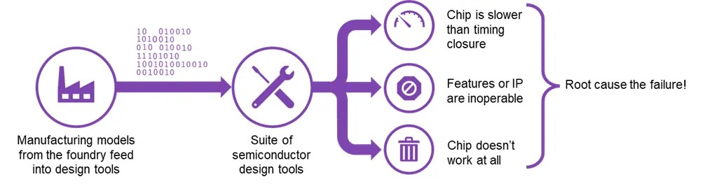
Fig. 1: Typical chip issues encountered in first silicon.
As a yield or product engineer, you need to understand exactly what’s going on inside the chip to try to debug the root cause of these problems. To help do that, embedded SLM in-chip monitor IP is typically leveraged. Along with the process monitor, voltage and temperature monitors (PVT) can provide critical information for root cause analysis.
While PVT monitors serve a tremendous purpose, the use of process detectors and their ability to help measure the power and performance of your chip device is becoming critical in today’s advanced SoCs. Analytics derived from voltage monitors can detect specific voltage droops in your chip and directly correlate to specific test failures on the tester. Similarly, analytics from thermal sensors can detect thermal gradients in your chip (e.g. one area of your chip running hotter than the rest of the chip) and correlate to specific test failures from the tester and further assist in the root cause of the failure.
However, process detectors are used for measuring the process health of your chips. They are hard IP designed for each individual process node of a given foundry. They are structured to form various ring oscillator (RO) chains which are simple, self-contained, homogeneous logic clusters placed in your design that are made up of inverters, NAND, or NOR standard cells. For example, a ring oscillator using inverter standard cells is comprised of an odd number of inverters connected in series from output to input repeatedly until the output of the last cell is connected to the input of the first cell. When the device is turned on, it oscillates, as its name implies. These ring oscillator chains will run as fast as they can and are self-limiting. If you have healthy silicon, they will run very fast and if you have unhealthy silicon, they will run very slow.
The data obtained from these monitor devices are typically charted manually and compared against the pre-silicon timing models from the foundry. In extreme cases, you may encounter timing issues such as hold time violations such as if the actual silicon is faster than the timing model or when the silicon operates slower than the required performance of the chip. In both cases, monitor analytics can perform further root cause and identify the cell(s) causing these timing issues. Additionally, there is the ability to be opportunistic in the case where you are well within your performance range, but the design has been over-margined allowing you to further reduce its power consumption by derating to slower cells while still meeting the performance requirements.
A newer type of embedded monitor, the path margin monitor (PMM), is becoming widely adopted. These monitors enhance the quality of results for measuring your silicon’s characteristics by measuring the slack of specific functional logic paths during manufacturing tests and in the field. However, unlike process detectors which are hard IP and are placed peripherally around the die of your chip, PMMs are soft IP that can be synthesized into the design independent of the process node and placed adjacent to any logic paths you define in your design. By periodically measuring the slack or margin of the paths, PMMs enable you to assess how the device is aging over its lifetime. As the device ages, the margin of the device may degrade and the data from PMMs will indicate that either the frequency or operating voltage needs to be adjusted to prolong the life of the device or enable you to identify and recall all devices that are progressively getting closer to failure before the device fails.
The analysis of the data collected from in-chip monitors has historically been a very manual and slow process. Reams of data are typically collected, stored and then downloaded from a database. The engineer must then spend hours manually pivoting, merging and stacking a dataset to create some charts where they need to personally assess and determine if there are any issues requiring corrective action. It is a cumbersome and slow process which must be performed repeatedly. It is performed while the chip is brought up in the early new product introduction (NPI) stage and after the chip is in a sustaining mode during high volume manufacturing (HVM) to observe how the chip is operating over time. Therefore, the goal for monitor analytics is to take this cumbersome analysis process and automate it and provide actionable information with only the push of a button – reducing the engineering time from hours to minutes.
However, to automate the process, you need several things to come together in a single analytics solution as follows:
Figure 2, shown below, is the result of an automated gap-to-target analysis. It is a standard funnel plot depicting one RO chain with the same physical characteristics from within all produced chips tested at several different voltages and compared against the simulated design target from the foundry. Effectively, the measured result from the tester is taken and divided by the TT (Typical, Typical) target where TT represents the typical PMOS and typical NMOS simulated timing results. Also shown is the FF (Fast, Fast) target and the SS (Slow, Slow) target to complete the bounds of the funnel. Both the FF and SS targets are also divided by the TT target to generate their position in the funnel plot.

Fig. 2: Funnel plot of a single ring oscillator chain tested at three (3) different voltages.
In a perfect world, if there is no variation or skew, you would see all the tested silicon measuring on the teal-colored TT line. However, in this example, as you increase the voltage during testing, half of the population of silicon is running faster than the FF target which is indicative of a scan hold timing violation. Therefore, if you are experiencing scan chain failures on these specific devices you can already root cause this problem using this monitor analytics analysis.
In Figure 3 shown below, the monitor analysis has been expanded to include three (3) RO chains of uniquely different physical characteristics. They share the same number of fins, same gate type, and same load cap but different Vt (e.g. threshold voltage) style. They each have their own dedicated Vt style labeled as VT1, VT2, and VT3.

Fig. 3: Box plot showing analysis of three (3) unique RO chains with varying Vt.
The results show a larger skew between the RO chains at higher voltage where VT2 is roughly on target but VT3 is lagging. Such a skew is indicative of potential timing failures.
Additional analysis can be provided from a monitor analytics solution to perform exhaustive design of experiments (DOE) to see how various physical transistor characteristics can impact performance across several RO chains to determine which portion of the DOE is impacting gap to TT target the most.
For example, figure 4 below shows a multivariant DOE which performs a series of exhaustive physical experiments independently and confirms the findings shown in figure 3 that VT3 has a statistically significantly higher gap-to-target than VT2. Moreover, correlations across all experiments show that Vt style affects gap-to-target more than fins, gate type, etc.
Figure 4 also incorporates a regression tree. A regression tree is a statistical method that will split the continuous variable, in this case gap-to-target, by categorical variables. The categorical variables are the RO DOE – all the physical characteristics that make up the RO. After all the experimental permutations across the entire population of chips is performed, it will indicate which categorical variable (e.g. physical attribute) drives the biggest delta across the population. In this example, Vt type caused the biggest gap-to-target. As a possible corrective action, if you have a critical path and you suspect a negative slack condition or experience a failure in silicon and you think the failing path is caused by VT3, you can do a VT swap by changing out the VT3 cell with the VT2 cell since the VT2 performance is more predictable than VT3.

Fig. 4: Multivariant DOE determines which physical characteristics impact gap to TT target the most.
There are many more examples of automation made possible by a monitor analytics solution for performing process classification of your silicon and too many to enumerate here. Figure 5 shows what a typical analytics cockpit might look like where you have many different analyses to select from and view.

Fig. 5: Process classification analysis performed by Silicon.da Monitor Analytics.
Process classification, however, is just one primary use case that you can perform using monitor analytics. There are many other use cases as well, such as Vmin prediction.
Vmin prediction is gaining adoption because of the benefits it provides. Firstly, identifying the lowest voltage that a device can run at and still meet the required performance has tremendous value. The lower the voltage you can run, the lower the power your device consumes which does two important things – (1) extends the performance of the device (e.g. cellphone) and (2) ultimately prolongs the life of the device. However, while this is of critical importance, it is not easy to attain since every individual device has its own unique minimum operating voltage. Hence, to derive the true Vmin of each device requires a lot of manufacturing testing which correlates to a lot of tester time thereby affecting time-to-market and, subsequently, higher test costs. Thus, if there is a way to closely predict the true Vmin without all of the extensive tester time and test costs, it would provide tremendous value to the developer of the device.
While predicting Vmin has been attempted throughout the years, not all methodologies are effective. Several key elements are required in order to provide an accurate Vmin prediction model – (1) Machining Learning (ML) model robustness, (2) actual measured Vmin from a sampling of devices to help train the model, and (3) data from monitor IP such as PVT and PMM as discussed earlier to provide more characteristics of the device to aid in the accuracy of the model.
Figure 6 below shows the difference between the accuracy of two different Vmin prediction models. The better prediction model will have a tighter correlation between what is measured and what is predicted (right side of the diagram). The best scenario is to have a model that predicts exactly what would have been measured (x=y).

Fig. 6: Two Vmin prediction models of varying accuracy.
In this figure, all the devices shown below the x=y line would pass since the predicted Vmin was either the same or higher than the measured Vmin for that device. Those devices above the line would fail since the predicted value is less than the measured value. To ensure a high enough yield of passing devices plus also factoring in a small percentage to compensate for the aging of the device, there should be a small increase in voltage (e.g. guard band) added to the predicted Vmin value. However, before offsetting the voltage, if a majority of the devices are already passing, an additional guard band may not be necessary. Further measured Vmin testing can be performed to reach an optimum Vmin in this case with the predicted Vmin used as the starting point for further testing.
To put this Vmin prediction model to practical use, figure 7 shows the procedural steps one would take to institute a Vmin prediction model in production.
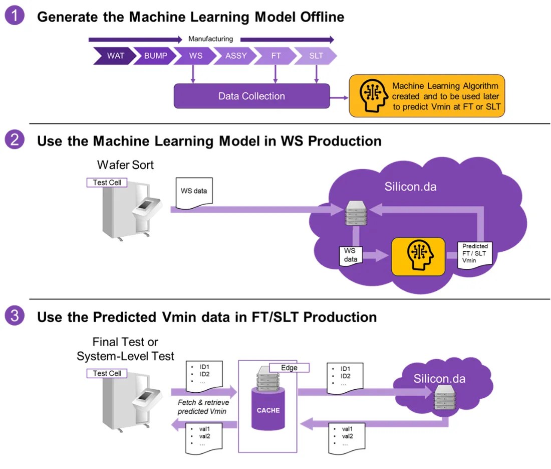
Fig. 7: Procedural steps for Vmin prediction.
The first step shown is to create and train the ML model on a predetermined set of devices. Note that actual measured Vmin testing needs to be done and the subsequent collected measured Vmin data used as a key contributor to train the model.
The second step is to apply the model on production data collected during wafer sort on the next batch of new silicon. Note that Vmin testing is no longer needed to be performed as the ML model will now be predicting the Vmin value to be used during FT and/or SLT. The predicted Vmin will be stored offline in memory until which time it is needed during FT or SLT.
The third and final step utilizes the predicted Vmin during FT or SLT. The engineers managing the testing can either leave the predicted Vmin as the final Vmin to be used in the end product or the Vmin predicted values can be used as a starting point for further measured Vmin testing if they would like to improve upon their results. However, the predicted values are at least a good approximate starting point, which still saves a lot of test time.
Visibility into complex SoCs is paramount to monitor and maintain the device’s health throughout its life and improve key operational metrics such as power and performance. Without it, you are flying blind and can only improve with excessive engineering and testing costs. Visibility from monitor data and automated insights from data analytics is a must for efficiently accomplishing these critical KPIs.
For further information on monitor analytics and high valued use cases, visit https://www.synopsys.com/ai/ai-powered-eda/silicon-da.html or contact your local salesperson.
 |
 |
 |
 |
 |
 |
 |
Leave a Reply